Detection panel and manufacturing method thereof, and photoelectric detection device

A manufacturing method and panel technology, applied in the direction of measuring devices, radiation control devices, circuits, etc., can solve the problems of reducing pixel sensitivity and loss, and achieve the effect of improving the sensitivity of the photoelectric effect and the level of pixel sensitivity

Active Publication Date: 2020-02-14
BOE TECH GRP CO LTD +1
View PDF5 Cites 2 Cited by
  • Summary
  • Abstract
  • Description
  • Claims
  • Application Information

AI Technical Summary

Problems solved by technology

[0004] Embodiments of the present invention provide a detection panel, its manufacturing method and detection device, which are used to solve the problem of loss of visible light in the prior art due to the fact that visible light will pass through the gap between the photodiode and the surrounding wiring to penetrate the pixel plane, and then pass through the transparent TFT substrate. out, thereby reducing the pixel sensitivity problem

Method used


Image

  • Detection panel and manufacturing method thereof, and photoelectric detection device
  • Detection panel and manufacturing method thereof, and photoelectric detection device
  • Detection panel and manufacturing method thereof, and photoelectric detection device

Examples


Embodiment Construction

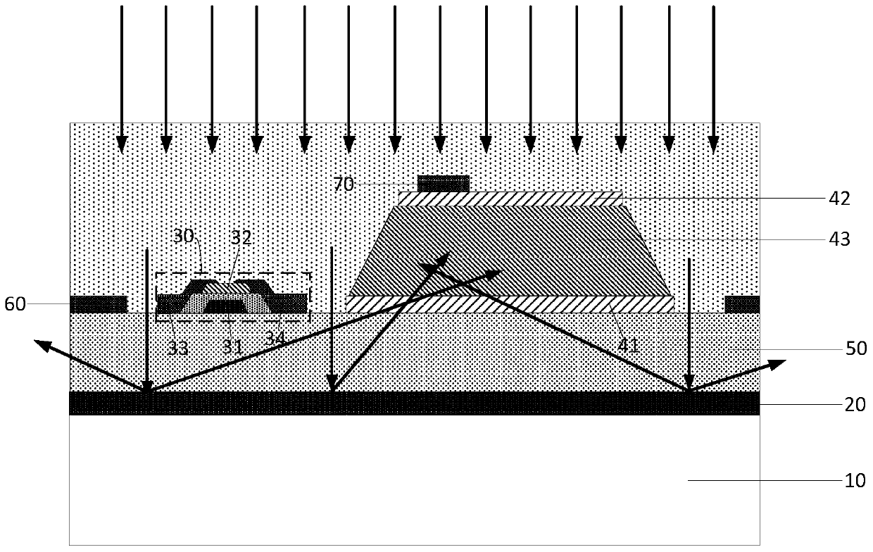
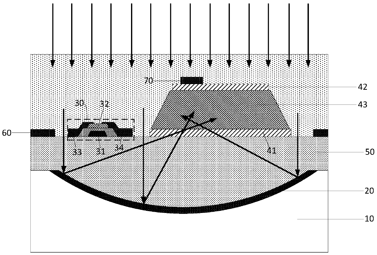
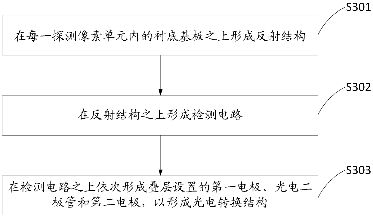
[0033] In order to make the object, technical solution and advantages of the present invention more clear, the specific implementations of the detection panel, its manufacturing method and detection device provided by the embodiments of the present invention will be described in detail below with reference to the accompanying drawings.

[0034] The thickness and shape of each layer of film in the drawings do not reflect the real scale of the detection panel, and the purpose is only to illustrate the content of the present invention.

[0035] At present, improving the visible light utilization rate of FPXD pixels is an important technical direction to improve image signal-to-noise ratio and reduce X-ray radiation dose. The current trend of mainstream pixel design improvement mainly revolves around increasing the filling rate of photodiodes in pixels to further increase the photosensitive area. But in fact, under the premise that the filling rate of the photodiode in the pixel i...


PUM


Abstract

The invention discloses a detection panel and a manufacturing method thereof, and a photoelectric detection device. According to the invention, a reflection structure is arranged between a substrate in each detection pixel unit and a detection circuit, when visible light enters the detection pixel unit area, the visible light is emitted, the reflection structure can reflect the visible light penetrating through the pixel plane from a gap between a photodiode and the peripheral wiring to the photodiode area, as a first electrode in the photoelectric conversion structure is a light-transmittingelectrode, the visible light reflected back to the photodiode area can be absorbed by the photodiode again, so the visible light penetrating through a pixel plane from the gap between the photodiode and the peripheral wiring is effectively utilized, photoelectric effect sensitivity of the pixel can be remarkably improved on the premise of not influencing the resolution, and the pixel sensitivity level in the prior art can be remarkably improved.

Description

technical field [0001] The invention relates to the technical field of detection panels, in particular to a detection panel, a manufacturing method thereof and a photoelectric detection device. Background technique [0002] Flat X-ray Panel Detector (FPXD) based on thin film transistor (Thin Film Transistor, TFT) technology is a crucial component in digital imaging technology, because of its fast imaging speed, good space and With the advantages of density resolution, high signal-to-noise ratio, and direct digital output, it is widely used in medical imaging (such as X-ray chest X-ray), industrial inspection (such as metal flaw detection), security inspection, air transportation and other fields. [0003] In the existing FPXD, it usually includes a detection panel for detecting X-rays, each detection panel includes a plurality of detection pixel units, and a photodetection readout circuit is set in the detection pixel unit to convert the optical signal into an electrical sig...

Claims


Application Information

Patent Timeline
Patent Type & Authority Applications(China)
IPC IPC(8): H01L27/146G01T1/20
CPCH01L27/14629H01L27/14663H01L27/14683G01T1/2018H01L27/14692H01L27/14636H01L27/14685H01L31/022475H01L31/105
Inventor 张冠尚建兴
Owner BOE TECH GRP CO LTD
Why Eureka
Try Eureka