
Developing pre-alignment machine with edge protection and double buckles for semiconductor wafer manufacturing

A pre-aligner, semiconductor technology, used in semiconductor/solid-state device manufacturing, electrical components, circuits, etc., can solve problems such as deviation of corners, easy sliding, and inability to develop normally

Inactive Publication Date: 2020-02-07
吴俊波
View PDF0 Cites 0 Cited by
  • Summary
  • Abstract
  • Description
  • Claims
  • Application Information

AI Technical Summary

Problems solved by technology

[0004] Aiming at the deficiencies in the prior art, the purpose of the present invention is to provide a semiconductor wafer manufacturing and developing pre-alignment machine with border protection and double buttons, so as to solve the problem of the prior art that the surface of the wafer itself is damaged while developing. It has a relatively smooth structure. When it is placed on the work surface, it needs to be fixed and corrected by the staff to carry out the developing operation. However, when it is fixed and corrected under the action of external force, its corners will be deviated or cannot be developed normally. , and at the same time, it is easy to slide under the slight shaking of the equipment, which requires manpower to continuously correct and fix it, and the process is relatively cumbersome.

Method used


Image

  • Developing pre-alignment machine with edge protection and double buckles for semiconductor wafer manufacturing
  • Developing pre-alignment machine with edge protection and double buckles for semiconductor wafer manufacturing
  • Developing pre-alignment machine with edge protection and double buckles for semiconductor wafer manufacturing

Examples


Embodiment Construction

[0026] In order to make the technical means, creative features, goals and effects achieved by the present invention easy to understand, the present invention will be further described below in conjunction with specific embodiments.

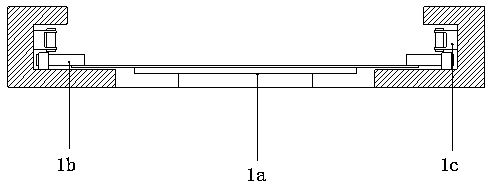
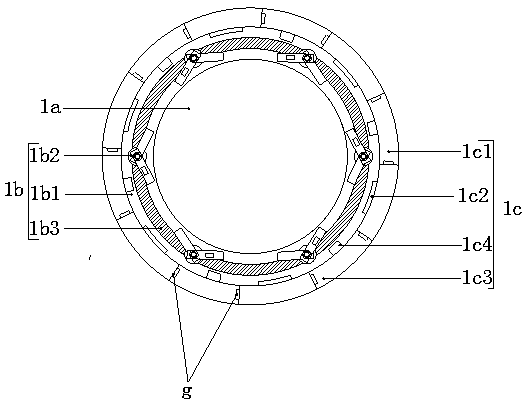
[0027] Such as Figure 1-Figure 5 As shown, the present invention provides a technical solution of a semiconductor wafer manufacturing development pre-alignment machine with frontier protection and double buttons:

[0028] Such as Figure 1-Figure 3 As shown, a semiconductor wafer manufacturing development pre-alignment machine with border protection and double buckles, its structure includes a double buckle protection device 1, a main body 2, a control panel 3, a support rod 4, a cover plate 5, and a developing optical device 6. The double buckle protection device 1 is set on the upper surface of the main body 2 and connected by electric welding. The control panel 3 is embedded in the front surface of the main body 2 and connected by electric we...


PUM


Abstract

The invention discloses a developing pre-alignment machine with edge protection and double buckles for semiconductor wafer manufacturing. The developing pre-alignment machine structurally comprises adouble-buckle fixed protection device, a machine body, a control panel, supporting rods, a cover plate and a developing light device. A wafer is buckled through cooperation of concave buckle plates and isolation air frames under dual protection effects of an adsorption air flow and soft cushions on the corners of the wafer, so that the wafer will not be twisted or even broken due to local shakingduring development in the oscillation process of equipment. The wafer is tightly buckled by corner buckle structures and magnetic strips under the action of an airbag ring, so that the deviation of development due to sliding of the wafer with a smooth structure is avoided.

Description

technical field [0001] The invention relates to the field of semiconductor manufacturing operations, more specifically, a semiconductor wafer manufacturing development pre-alignment machine with border protection and double buttons. Background technique [0002] The raw material of the wafer is silicon. With the continuous improvement of its manufacturing process, the wafer is widely used in various circuit component structures. When the wafer is manufactured, it needs to melt a lot of silicon, and then melt it The seed crystal is planted in the liquid, and then slowly pulled out to form a cylindrical single crystal silicon rod, which can be cut, rolled, sliced, chamfered, polished, laser engraved (developed), and then processed Packaging, because it is used in circuit components, has strict control on the manufacturing process. When developing it, it needs to use equipment to pre-calibrate the wafer to ensure the standard development of the wafer. . [0003] However, at t...

Claims


Application Information

Patent Timeline
Patent Type & Authority Applications(China)
IPC IPC(8): H01L21/687
CPCH01L21/68721H01L21/68728H01L21/68735H01L21/68785
Inventor 吴俊波
Owner 吴俊波
Learn More