PCB detection and wiping integrated machine

A technology of PCB board and all-in-one machine, applied in the field of PCB board detection and wiping all-in-one machine, can solve the problems of PCB board gold finger damage, increase production cost, insecurity, etc., to speed up production efficiency, improve effect, and save production cost. Effect

Active Publication Date: 2020-02-07
SUZHOU CHOUCE ELECTRONICS TECH
View PDF11 Cites 13 Cited by
  • Summary
  • Abstract
  • Description
  • Claims
  • Application Information

AI Technical Summary

Problems solved by technology

[0005] First, it is not safe to manually wipe the PCB board from left to right across the alcohol-stained sponge and the dry sponge, because the angular speed of the sponge depends on human operation, so it is easy to wipe the PCB board. The golden finger is broken, and the wiping efficiency is low;
[0006] Second, not every gold finger on the PCB needs to be wiped, and when manual wiping is used, it is difficult to distinguish the difference between the circuit boards that need to be wiped or the circuit boards that do not need to be wiped by the naked eye, so all wiping is usually used. practice, and all wiping not only increases the labor intensity of the staff, but also increases the production cost

Method used


Image

  • PCB detection and wiping integrated machine
  • PCB detection and wiping integrated machine
  • PCB detection and wiping integrated machine

Examples


Embodiment

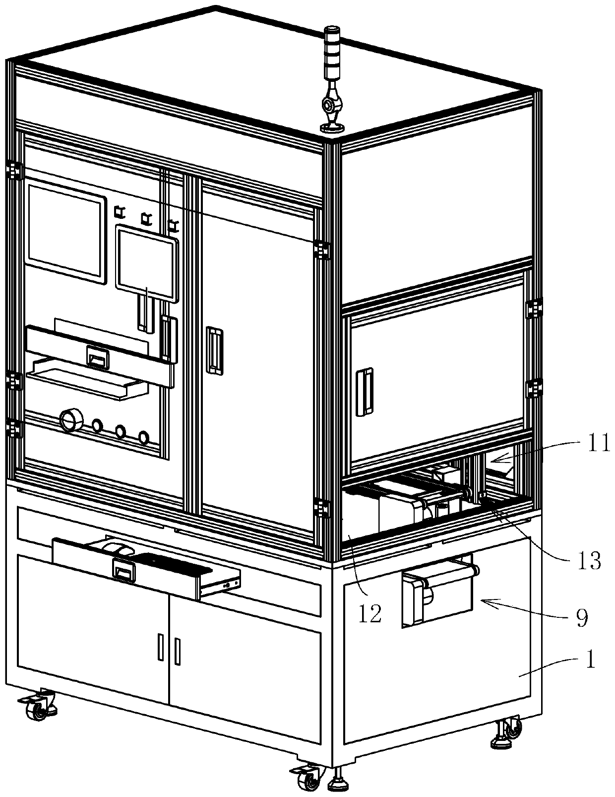
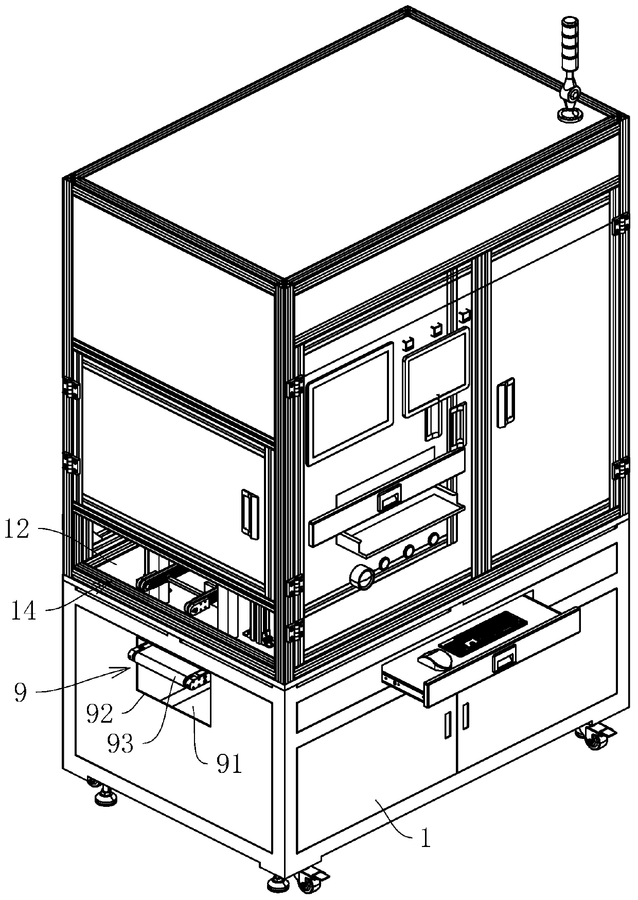
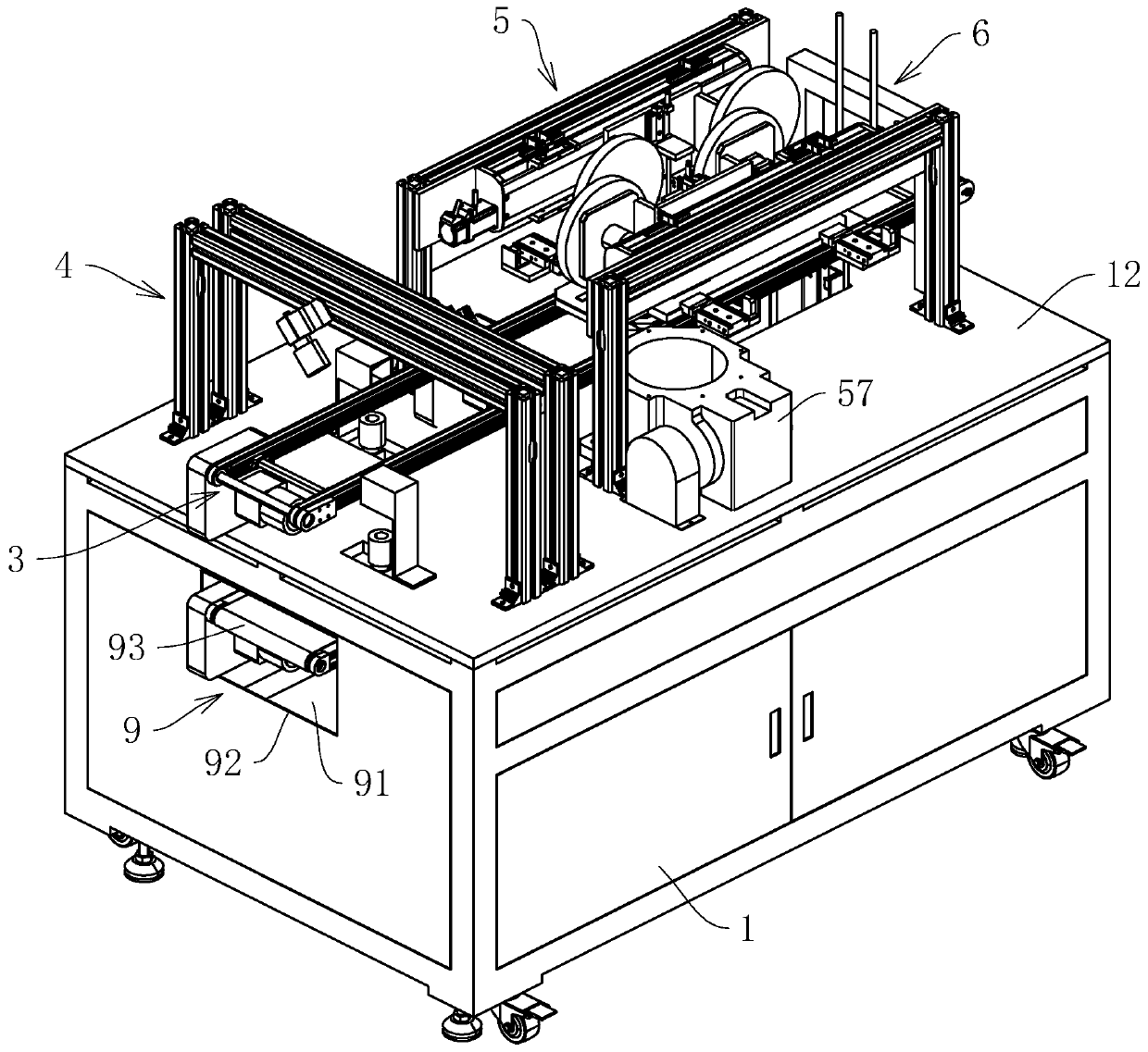
[0054] refer to figure 1 and figure 2 , is a PCB inspection and wiping all-in-one machine disclosed in the present invention, including a housing 1 and a workbench 12 horizontally arranged in the housing 1, the workbench 12 divides the inside of the housing 1 from top to bottom into a working chamber 11 And the installation cavity 91. One end of the housing 1 is provided with a material inlet 13 communicating with the working chamber 11 , and the other end of the housing 1 is provided with a material outlet 14 communicating with the working chamber 11 . The end of the housing 1 near the feed port 13 and the end near the discharge port 14 are both provided with a through port 92, and a return line 9 is provided in the installation cavity 91. Specifically, the return line 9 is provided in the installation cavity 91 The conveyor belt 93 is arranged along the direction from the feed port 13 to the discharge port 14, and both ends of the conveyor belt 93 protrude from the housin...


PUM


Abstract

The invention discloses a PCB detection and wiping integrated machine, relates to the technical field of PCB cleaning, and aims to solve the problems that an existing PCB gold finger cleaning machineis low in efficiency and unsafe. The key points of the technical scheme are that the PCB detection and wiping integrated machine comprises a workbench, a conveying mechanism, a detection component, awiping mechanism, and a blowing device, wherein the workbench is horizontally arranged in a shell, one end of a machine body is provided with a feeding port, and the other end of the machine body is provided with a discharging port; the conveying mechanism is supported by the workbench and used for conveying a PCB from the feeding port to the discharging port; the detection component is arranged at the end, close to the feeding port, of the workbench and used for detecting gold fingers of the PCB; the wiping mechanism is supported by the workbench and used for wiping the gold fingers of the PCB; and the blowing device is arranged at the end, close to the discharging port, of the workbench and used for blowing and drying the gold fingers of the PCB. The wiping mechanism operates in responseto a detection signal output by the detection component, the blowing device operates in response to an action signal output by the wiping mechanism, and the PCB detection and wiping integrated machine has the effects of being safe, efficient and beneficial to reducing the production cost.

Description

technical field [0001] The invention relates to the technical field of PCB board cleaning, in particular to a PCB board detection and wiping all-in-one machine. Background technique [0002] The golden finger is composed of multiple golden conductive contacts, which are set on the circuit board to transmit signals. Because the surface of the conductive contacts on the PCB is gold-plated and the conductive contacts are arranged like fingers, they are called "golden fingers". After low-pressure injection molding in wire harness processing, since the golden fingers of the PCB board may be dirty, it needs to be wiped and cleaned with alcohol to ensure its signal transmission performance. [0003] The Chinese patent with the existing authorized notification number CN206838570U discloses a PCB gold finger cleaning machine, including a water pipe and a base, and the syringe is connected with the dispensing machine, and the dispensing machine is installed on the top right side of t...

Claims


Application Information

Patent Timeline
IPC IPC(8): B08B1/00B08B1/02B08B13/00F26B21/00G01N21/956
CPCB08B13/00F26B21/004G01N21/956G01N2021/95638B08B1/20B08B1/143
Inventor 王怀军柴先接
Owner SUZHOU CHOUCE ELECTRONICS TECH
Why Eureka
Try Eureka