
Wafer cleaning device

A technology for cleaning devices and wafers, which is applied in the manufacture of electrical components, circuits, semiconductors/solid-state devices, etc. It can solve the problems of cumbersome wafer cleaning steps, cumbersome cleaning steps, and low cleaning efficiency, and save the time for flipping and transferring , Enhance the cleaning effect and improve the cleaning efficiency

Active Publication Date: 2020-01-17
YANGTZE MEMORY TECH CO LTD
View PDF16 Cites 3 Cited by
  • Summary
  • Abstract
  • Description
  • Claims
  • Application Information

AI Technical Summary

Problems solved by technology

[0004] In the prior art, the wafer cleaning steps are very cumbersome. It is necessary to take out the wafer from the front opening unified pod (FOUP), turn the wafer over so that the back of the wafer faces upward, and put it into the first cleaning chamber. Clean the back of the wafer in the second cleaning chamber; then, take the wafer out, turn it over again so that the front of the wafer is facing up, put it into the second cleaning chamber, and clean the front of the wafer
Due to the cumbersome cleaning steps, the cleaning efficiency is very low, and when the wafer is turned over, it is easy to misuse, which makes the orientation of the wafer wrong, which affects the progress of the subsequent process
[0005] In addition, since the pollutants on the back of the wafer may adhere to the wafer, it is not easy to completely remove the pollutants, which will affect the focus of the subsequent photolithography process

Method used


Image

  • Wafer cleaning device
  • Wafer cleaning device

Examples


Embodiment Construction

[0023] Hereinafter, the present invention will be described in more detail with reference to the accompanying drawings. In the various figures, identical elements are indicated with similar reference numerals. For the sake of clarity, various parts in the drawings have not been drawn to scale. Also, some well-known parts may not be shown in the drawings.

[0024] In the following, many specific details of the present invention, such as structures, materials, dimensions, processes and techniques of components, are described for a clearer understanding of the present invention. However, the invention may be practiced without these specific details, as will be understood by those skilled in the art.

[0025] It should be understood that when describing the structure of a component, when a layer or a region is referred to as being "on" or "over" another layer or another region, it may mean being directly on another layer or another region, or Other layers or regions are also in...


PUM


Abstract

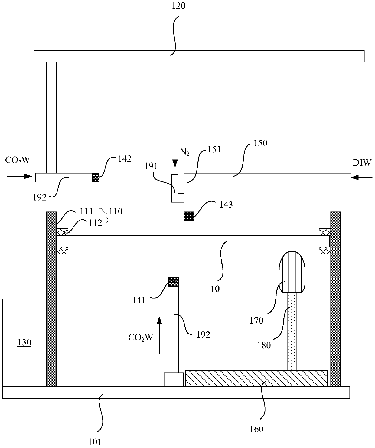
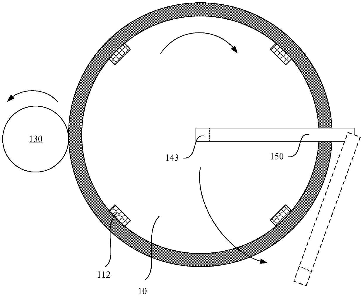
The invention discloses a wafer cleaning device, and the device comprises a wafer placing mechanism which is used for clamping the edge of a wafer and driving the wafer to rotate; a first spray head which is positioned on one side of the wafer placing mechanism and is used for upwards spraying a cleaning agent to the back surface of the wafer; and a cleaning brush and a guide rail which are located on one side of the wafer placing mechanism, wherein the cleaning brush is movably connected with the guide rail, and the cleaning brush can move relative to the guide rail and is used for cleaning the back of the wafer. When the wafer cleaning device is used for cleaning the back surface of the wafer, pollutants on the back surface of the wafer can be influenced by the shearing force of the cleaning brush and the gravity of the cleaning brush at the same time, so that the pollutants can be moved out of the back surface of the wafer more easily, and the cleaning effect is enhanced.

Description

technical field [0001] The present invention relates to the technical field of semiconductors, and more particularly, to a wafer cleaning device. Background technique [0002] The improvement of the storage density of the memory device is closely related to the progress of the semiconductor manufacturing process. As the feature size of the semiconductor manufacturing process becomes smaller and smaller, the storage density of the memory device becomes higher and higher. In order to further increase storage density, memory devices with a three-dimensional structure (ie, 3D memory devices) have been developed. A 3D memory device includes a plurality of memory cells stacked in a vertical direction, which can double the integration level on a wafer per unit area and reduce the cost. [0003] The size of 3D memory devices is getting smaller and smaller, and the requirements for the accuracy of photolithography steps are getting higher and higher. In order to ensure the accuracy...

Claims


Application Information

Patent Timeline
Patent Type & Authority Applications(China)
IPC IPC(8): H01L21/67H01L21/02
CPCH01L21/67046H01L21/67051H01L21/0209
Inventor 朱焜顾立勋夏余平
Owner YANGTZE MEMORY TECH CO LTD
Learn More