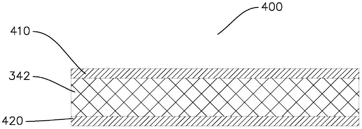
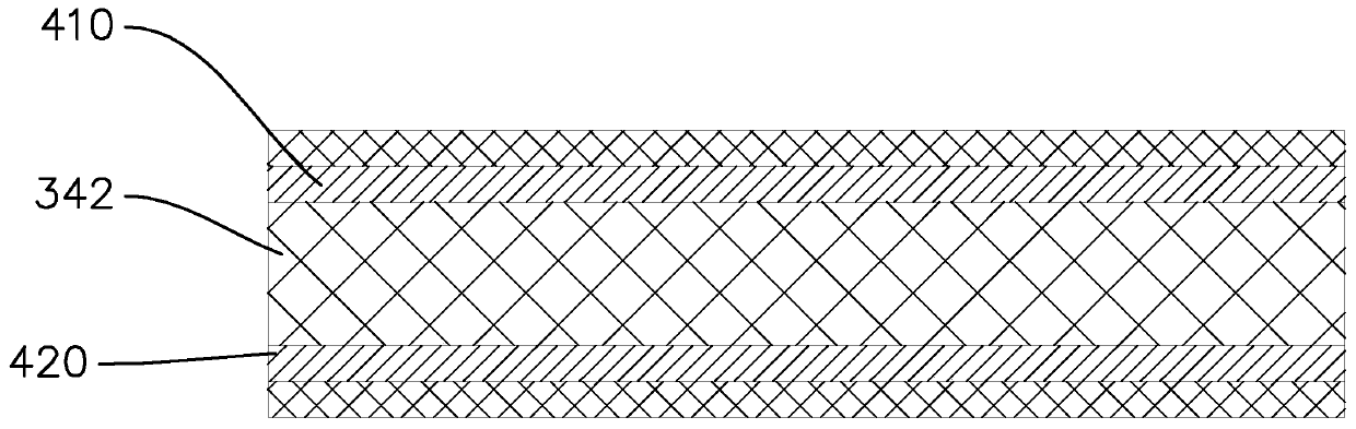
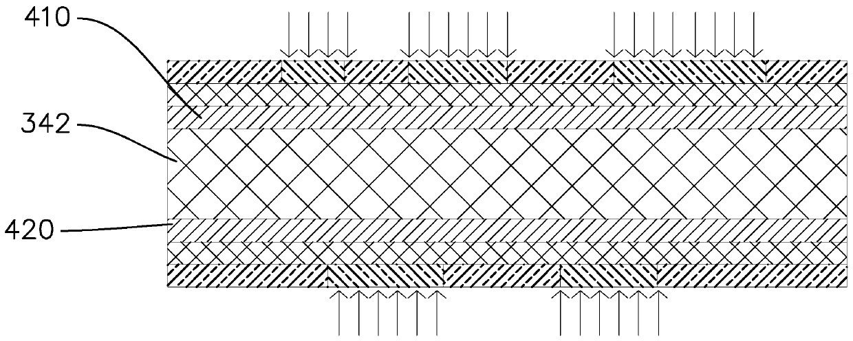
LED lamp panel and production process
A technology of LED lamp board and manufacturing process, which is applied in printed circuit manufacturing, instruments, electrical components, etc., can solve the problems of damage to LED lamp beads, cumbersome operation process, and inability to repair and replace LED lamp beads, so as to achieve convenient protection structure, Protecting the effect of technical effects
- Summary
- Abstract
- Description
- Claims
- Application Information
AI Technical Summary
Problems solved by technology
Method used
Image

Examples
Embodiment Construction
[0048] This part will describe the embodiment of the present invention in detail, and the embodiment of the present invention is shown in the accompanying drawings, and the function of the accompanying drawings is to supplement the description of the text part of the specification with figures, so as to be able to intuitively and vividly understand the embodiments of the present invention Each technical feature and the overall technical solution, but they should not be construed as limiting the protection scope of the present invention.
[0049] In the description of the present invention, if it involves orientation description, for example, the orientation or positional relationship indicated by "upper", "lower", "front", "back", "left", "right" etc. is based on the The orientation or positional relationship is only for the convenience of describing the present invention and simplifying the description, but does not indicate or imply that the device or element referred to must...
PUM
 Abstract
Description
Claims
Application Information
 - R&D
- Intellectual Property
- Life Sciences
- Materials
- Tech Scout
- Unparalleled Data Quality
- Higher Quality Content
- 60% Fewer Hallucinations
Browse by: Latest US Patents, China's latest patents, Technical Efficacy Thesaurus, Application Domain, Technology Topic, Popular Technical Reports.
© 2025 PatSnap. All rights reserved.Legal|Privacy policy|Modern Slavery Act Transparency Statement|Sitemap|About US| Contact US: help@patsnap.com