Method for preparing array substrate and display panel

A technology of array substrates and substrates, applied in semiconductor devices, electrical components, circuits, etc., can solve the problems of process yield loss, complex structure, increased time cost, material cost, etc., and achieve cost saving, time saving, and cost saving Effect

Active Publication Date: 2022-05-31
SHENZHEN CHINA STAR OPTOELECTRONICS SEMICON DISPLAY TECH CO LTD
View PDF5 Cites 0 Cited by
  • Summary
  • Abstract
  • Description
  • Claims
  • Application Information

AI Technical Summary

Problems solved by technology

[0003] At present, the AMOLED top-gate thin-film transistor array substrate manufacturing process has complex structure and many manufacturing processes. As we all know, each additional array manufacturing process not only increases the time cost and material cost, but also is accompanied by the loss of process yield.

Method used


Image

  • Method for preparing array substrate and display panel
  • Method for preparing array substrate and display panel
  • Method for preparing array substrate and display panel

Examples


Embodiment

[0055] The preparation method of the array substrate 10 of the present invention includes the following steps:

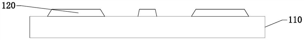
[0056] S1) Provide a substrate 110, the substrate 110 is a glass substrate, which is convenient to undertake subsequent thin film transistor manufacturing processes.

[0057] S2) As shown in FIG. 1, a layer of light-shielding layer 120 is prepared on the substrate 110, and the light-shielding layer 120 is a high-reflection gold

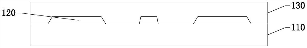
[0058] S3) As shown in FIG. 2 , a first insulating layer 130 is covered on the light shielding layer 120, because the light shielding layer 120

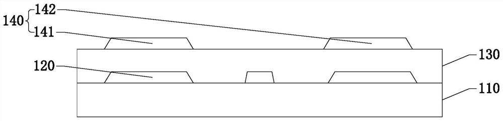
[0059] S4) As shown in FIG. 3, a layer of IGZO layer 140 is formed on the first insulating layer 130, which is formed by a patterning process

[0060] S5) As shown in FIG. 4, a second insulating layer 150 is formed on the first insulating layer 130, and the second insulating layer

[0061] S6) As shown in FIG. 5, a photoresist layer 160 is formed on the second insulating layer 150 through a mask, and th...


PUM


Abstract

The invention discloses a preparation method of an array substrate and a display panel, wherein the preparation method of the array substrate comprises the following steps: S1) providing a substrate; S2) preparing a light-shielding layer on the substrate; S3) forming a light-shielding layer on the light-shielding layer Covering a first insulating layer; S4) forming a layer of IGZO layer on the first insulating layer, forming an active layer and an anode layer through a patterning process; S5) forming a second layer on the first insulating layer an insulating layer, the second insulating layer covers the IGZO layer. The beneficial effect of the present invention is that the preparation method of the array substrate and the display panel of the present invention prepare the first insulating layer and the second insulating layer through a photomask, which saves the cost of the photomask, and uses the same material to prepare the active layer and the second insulating layer at the same time. The anode layer is made of highly reflective metal to make the light-shielding layer, which not only achieves the purpose of light-shielding, but also can be used as pixel wiring, which reduces the multi-channel array process in the prior art to only 5-channel array process, which not only saves time but also Cost savings.

Description

Method for preparing an array substrate and display panel technical field [0001] The present invention relates to the field of display, and in particular, to a method for preparing an array substrate and a display panel. Background technique AMOLED (English: Active-matrix organic light-emitting diode, Chinese translation: active matrix Organic Light Emitting Diodes or Active Matrix Organic Light Emitting Diodes) is a display technology. OLED (Organic Light Emitting Diode) Body) is a specific type of thin film display technology: organic electroluminescence display; AM (active matrix body or active matrix) body) refers to the underlying pixel addressing technology. At present, AMOLED technology is mainly used in smartphones, and continues to move towards low power consumption and low cost. This and large-scale development. [0003] At present, the AMOLED top-gate thin film transistor array substrate manufacturing process is complicated in structure and has many manu...

Claims


Application Information

Patent Timeline
Patent Type & Authority Patents(China)
IPC IPC(8): H01L27/12H01L27/32
CPCH01L27/1288H10K59/12
Inventor 唐甲任章淳
Owner SHENZHEN CHINA STAR OPTOELECTRONICS SEMICON DISPLAY TECH CO LTD
Why Eureka
Try Eureka