Automatic copper deposition control process for printed circuit board

An automatic control and printed circuit board technology, which is applied in the direction of printed circuit, printed circuit manufacturing, and electrical connection formation of printed components, etc., can solve the problems of product quality risk, inability to adjust in time, and long time spent, etc., to achieve stable backlight Quality, save material cost, improve the effect of accuracy

Active Publication Date: 2019-11-15
福州瑞华印制线路板有限公司
View PDF4 Cites 3 Cited by
  • Summary
  • Abstract
  • Description
  • Claims
  • Application Information

AI Technical Summary

Problems solved by technology

Due to the following defects in the traditional backlight judgment: 1. Destructive test, the hole needs to be ground to the hole radius with a grinder, and the light is irradiated with a metal microscope to see the degree of light transmission in the hole. The place covered by the sunken copper layer is not transparent. Light, according to the backlight progression table to judge, this process is a qualitative judgment, the accuracy is not high; 2, according to the backlight judgment and then adjust the copper sinking parameters, because the backlight judgment process requires grinding and other operations, it takes a long time 3. In the process of determining the backlight, if the potion fails, the produced board cannot be adjusted in time, and the quality risk of the outflowing product exists

Method used


Image

  • Automatic copper deposition control process for printed circuit board
  • Automatic copper deposition control process for printed circuit board
  • Automatic copper deposition control process for printed circuit board

Examples


Embodiment Construction

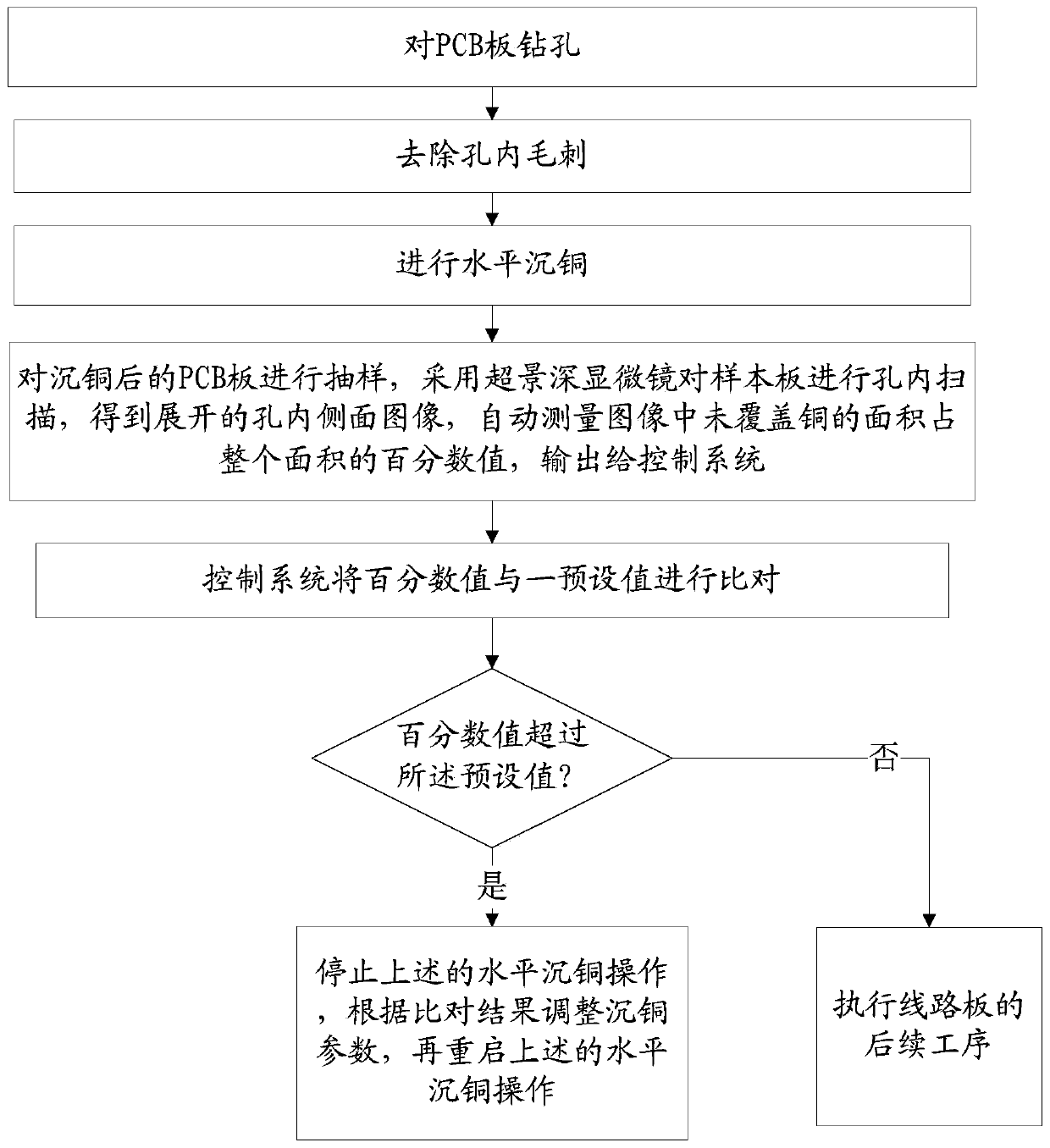
[0024] Such as Figure 1 to Figure 3 As shown, a printed circuit board automatic control copper sinking process of the present invention needs to provide an ultra-depth-of-field microscope and a control system. The ultra-depth-of-field microscope is connected to the control system and is controlled by the control system. The process includes the following steps:

[0025] Step 1. Drill holes on the PCB board;

[0026] Step 2. Remove the burr in the hole;

[0027] Step 3. Perform horizontal copper sinking; choosing horizontal copper sinking is more conducive to the realization of automated production lines than vertical copper sinking, because when horizontal copper sinking, PCB boards are circulated one by one through the scroll bar, rather than batch transmission like vertical copper sinking , and it is also convenient for the follow-up manipulator to randomly grab for sampling inspection.

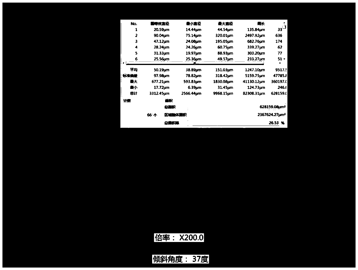
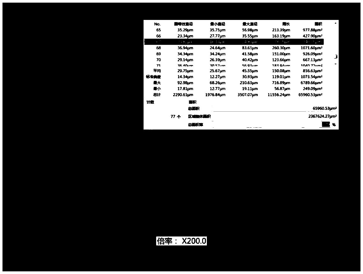
[0028] Step 4. Sampling the PCB board after sinking copper, scanning the inside of t...


PUM


Abstract

The invention provides an automatic copper deposition control process for a printed circuit board. A super scene depth microscope and a control system are required. The super scene depth microscope isconnected with the control system and controlled by the control system. The process comprises steps: drilling is carried out on the PCB; burrs in the hole are removed; horizontal copper deposition iscarried out; PCBs after copper deposition are sampled, the super scene depth microscope is adopted to perform in-hole scanning on sample boards, an unfolded in-hole side image is obtained, the percentage value of the area without copper covering in the image in the whole area is automatically measured, and the percentage value is outputted to the control system; if the percentage value exceeds apreset value, the above horizontal copper deposition operation is stopped, copper deposition parameters are adjusted according to a comparison result, and the above horizontal copper deposition operation is restarted; and if the percentage value does not exceed the preset value, the subsequent steps of the circuit board are performed. Through introducing a 3D imaging technology to circuit board making, quantitative detection of light transmission points is realized, the backlight determination accuracy and the detection speed are improved, industrial automation is realized, and the productionefficiency and the quality are improved.

Description

technical field [0001] The invention relates to the field of circuit board production, in particular to an automatic control copper sinking process of a printed circuit board. Background technique [0002] The traditional copper sinking process mainly includes sinking copper out of the board -> backlight judgment -> production control. Among them, sinking copper out of the board refers to sinking copper after drilling the PCB board. The sinking copper refers to electroless copper sinking (Plated Through Hole), that is, plated through hole, referred to as PTH, which is a process used in the production of printed circuit boards. It is an extremely important process, the purpose of which is to cover the non-conductor hole wall with a dense and firm metal copper layer as a conductor by means of chemical deposition, so that the lines between two or more layers of the circuit board are connected and conductive; backlight determination And production control means that after...

Claims


Application Information

Patent Timeline
Patent Type & Authority Applications(China)
IPC IPC(8): H05K3/42H05K3/00
CPCH05K3/42H05K3/0047H05K3/0055
Inventor 陈跃生李先强詹少华
Owner 福州瑞华印制线路板有限公司
Why Eureka
Try Eureka