Accelerator for GoogLeNet model and method thereof

An accelerator and model technology, applied in the field of neural network algorithms and optoelectronic computing, can solve the problems of gradient dispersion, high computational complexity, and difficulty in optimizing models, and achieve high energy efficiency and small size.

Active Publication Date: 2019-09-27
NANJING SIMIND SEMICON LTD
View PDF4 Cites 3 Cited by
  • Summary
  • Abstract
  • Description
  • Claims
  • Application Information

AI Technical Summary

Problems solved by technology

But this method has the following problems: (1) There are too many parameters, and if the training data set is limited, it is easy to produce overfitting; (2) The larger the network, the more parameters, the greater the computational complexity, and it is difficult to apply; (3) ) the deeper the network, the gradient dispersion problem is prone to occur (the gradient is easy to disappear as it traverses backwards), and it is difficult to optimize the model
However, due to the large size of the GoogLeNet model, the feature maps and weight data required for convolution operations and full connection operations are large, resulting in a huge energy consumption in data transmission, and the operation speed of traditional computing systems is slow.

Method used


Image

  • Accelerator for GoogLeNet model and method thereof
  • Accelerator for GoogLeNet model and method thereof
  • Accelerator for GoogLeNet model and method thereof

Examples


Embodiment 1

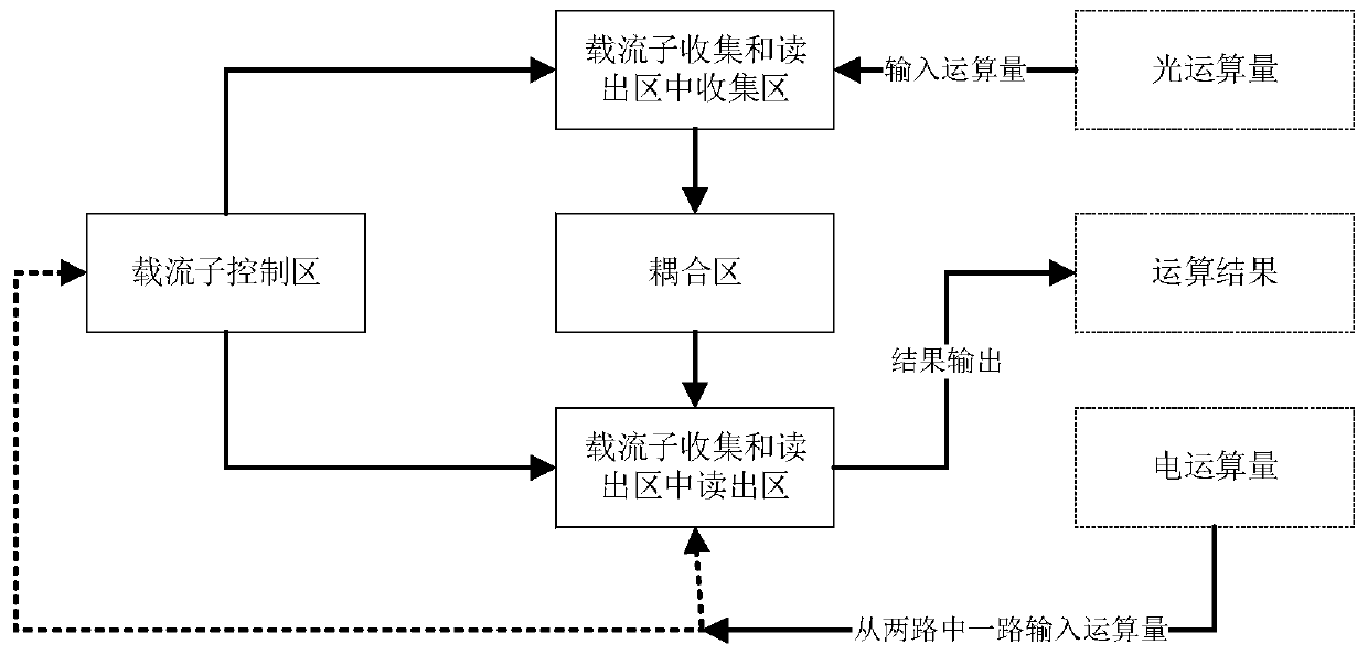
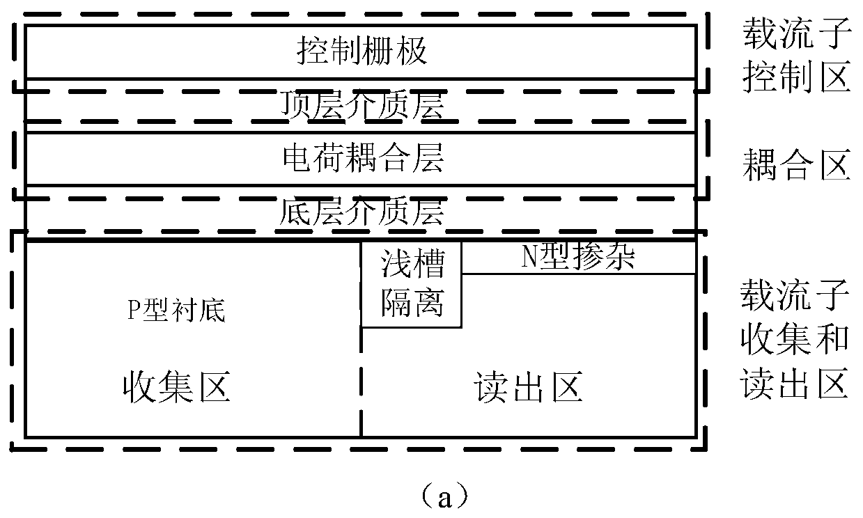
[0032] like image 3As shown, the computing unit of this embodiment includes: a control gate as a carrier control region, a charge coupling layer as a coupling region, and a P-type substrate as a photo-generated carrier collection region and a readout region. The substrate is divided into a left collecting area and a right reading area, wherein the right reading area includes shallow trench isolation, an N-type source terminal and an N-type drain terminal formed by ion implantation. The shallow trench isolation is located in the middle of the semiconductor substrate, between the collection area and the readout area. The shallow trench isolation is formed by etching and filled with silicon dioxide to isolate the electrical signals of the collection area and the readout area. The N-type source terminal is located on the side of the readout region close to the underlying dielectric layer, and is formed by doping by ion implantation. The N-type drain terminal is located on the ot...

Embodiment 2

[0038] like Figure 4 As shown, the computing unit of this embodiment includes: a control gate as a carrier control region, a charge coupling layer as a coupling region, and a P-type semiconductor substrate as a photo-generated carrier collection region and a readout region, wherein The P-type substrate includes an N-type source terminal and a drain terminal formed by ion implantation. The P-type semiconductor substrate can undertake the work of photosensitive and readout at the same time. The N-type source terminal is located on the side of the readout region close to the underlying dielectric layer, and is formed by doping by ion implantation. The N-type drain terminal is located on the other side of the semiconductor substrate near the underlying dielectric layer and opposite to the N-type source terminal, and is also formed by doping by ion implantation.

[0039] When photosensitive, a pulse with a negative voltage range is applied to the P-type semiconductor substrate, ...

Embodiment 3

[0044] like Figure 5 As shown, the computing unit of this embodiment includes: a photodiode and a readout tube serving as a collection and readout region of photogenerated carriers, wherein the photodiode is formed by ion doping and is responsible for light-sensing. The N region of the photodiode is connected to the control gate of the readout tube and the source end of the reset tube through the optoelectronic coupling lead as the coupling region, and a positive voltage pulse is applied to the drain end of the readout tube as the drive voltage of the readout current; exposure Before exposure, the reset tube is turned on, and the voltage of the drain terminal of the reset tube is applied to the photodiode, so that the photodiode as the collection area is in a reverse biased state, and a depletion layer is generated; during exposure, the reset tube is turned off, the photodiode is electrically isolated, and the photon After incident in the depletion region of the photodiode, p...


PUM


Abstract

The invention discloses an accelerator for a GoogLeNet model and a method thereof. The accelerator comprises: a controller which is used for controlling control signal flow and data flow of convolution operation and full connection operation and outputting and storing a final result in a memory; a photoelectric calculation array which is used for completing matrix vector multiplication operation after convolution operation and full connection operation mapping; an analog-to-digital converter which is used for converting the current output by the photoelectric calculation array into a digital signal; an activation function unit which is used for completing bias adding and activation function operation of convolution operation and full connection operation results; and a pooling unit which is used for completing the maximum pooling operation of the result. Convolutional operation and full connection operation of the GoogLeNet model are achieved based on the photoelectric computing array, the inference process of the GoogLeNet model can be effectively accelerated, and the method has the advantages of being high in energy efficiency, free of repeated access to off-chip storage and the like.

Description

technical field [0001] The invention relates to an accelerator of a GoogLeNet model based on an optoelectronic computing array and a method thereof, belonging to the field of optoelectronic computing and the field of neural network algorithms. Background technique [0002] Neural network is the current research hotspot in the field of artificial intelligence, and the most direct way to improve the performance of neural network is to increase the depth and width of the network, where the depth refers to the number of network layers, and the width refers to the number of neurons. But this method has the following problems: (1) there are too many parameters, if the training data set is limited, it is easy to over-fit; (2) the larger the network and the more parameters, the greater the computational complexity, and it is difficult to apply; (3) ) The deeper the network, the more prone to gradient dispersion problem (the gradient goes back and disappears easily), and it is diffic...

Claims


Application Information

Patent Timeline
Patent Type & Authority Applications(China)
IPC IPC(8): G06N3/04G06N3/063G06N3/067
CPCG06N3/063G06N3/0675G06N3/045
Inventor 王瑶席挺王宇宣
Owner NANJING SIMIND SEMICON LTD
Why Eureka
Try Eureka