Phase focusing image sensor and forming method and working method thereof
An image sensor and phase focusing technology, which is applied in image communication, electric solid-state devices, semiconductor devices, etc., can solve the problems of poor performance of image sensors, achieve the effect of improving performance and avoiding white spots
- Summary
- Abstract
- Description
- Claims
- Application Information
AI Technical Summary
Problems solved by technology
Method used
Image
Examples
Embodiment Construction
[0034] As mentioned in the background, the performance of prior art phase focusing image sensors is poor.
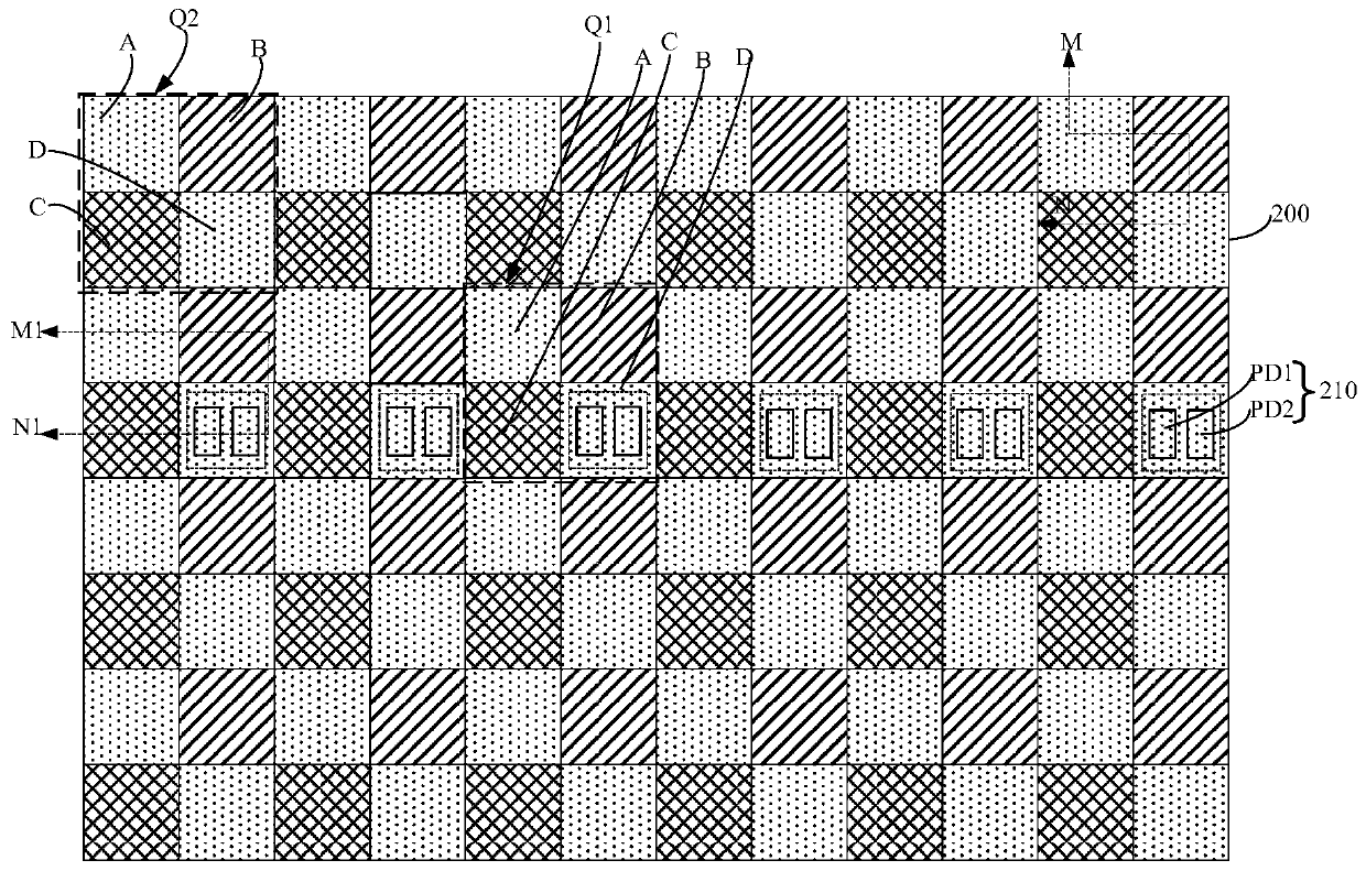
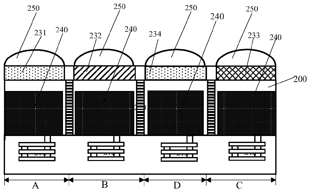
[0035] A phase focus image sensor, please refer to figure 1 , including: a semiconductor substrate 100, the semiconductor substrate 100 includes several sub-pixel regions; a focus photosensitive unit 110 located in the semiconductor substrate, the focus photosensitive unit 110 includes a first focus photosensitive structure 111 and a second focus photosensitive structure that are separated from each other Structure 112, one focusing photosensitive unit 110 is located in two adjacent sub-pixel areas, the first focusing photosensitive structure 111 is located in one sub-pixel area, and the second focusing photosensitive structure 112 is located in the other sub-pixel area; located in the first focusing The color of the filter layer on the photosensitive structure 111 is the same as that of the filter layer on the second focus photosensitive structure 112 .
[0036] exist ...
PUM
 Abstract
Description
Claims
Application Information
 - R&D
- Intellectual Property
- Life Sciences
- Materials
- Tech Scout
- Unparalleled Data Quality
- Higher Quality Content
- 60% Fewer Hallucinations
Browse by: Latest US Patents, China's latest patents, Technical Efficacy Thesaurus, Application Domain, Technology Topic, Popular Technical Reports.
© 2025 PatSnap. All rights reserved.Legal|Privacy policy|Modern Slavery Act Transparency Statement|Sitemap|About US| Contact US: help@patsnap.com


