Display panel, manufacturing method thereof, and display device
A technology for a display panel and a manufacturing method, which is used in the manufacture of semiconductor/solid-state devices, semiconductor devices, electrical components, etc., can solve the problem of inconsistent brightness of display panels, and achieve the advantages of improving uneven brightness display, increasing current flow, and reducing resistance. Effect
- Summary
- Abstract
- Description
- Claims
- Application Information
AI Technical Summary
Problems solved by technology
Method used
Image

Examples
Embodiment 1
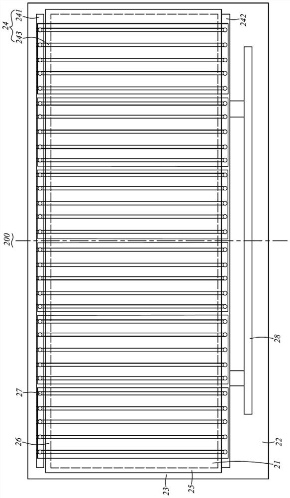
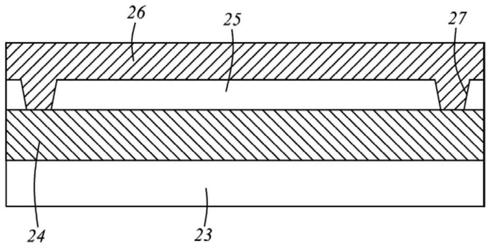
[0046] see figure 2 , which is a schematic diagram of the display panel 200 of the present invention. like figure 2As shown, the present embodiment provides a display panel 200, in which the second metal wiring is formed on the packaging film to increase the electrical parallel wiring of the display substrate, so that the display brightness of the display panel is uniform. The display panel 200 includes a display substrate 23 , a first metal trace 24 disposed on the display substrate 23 , a packaging film 25 disposed on the first metal trace 24 , and a packaging film 25 disposed on the packaging film 25 . an insulating layer (not shown), a second metal trace 26 disposed on the insulating layer, the display substrate 23 has a display area 21 and a non-display area 22 surrounding the display area 21, the first The metal traces 24 and the second metal traces 26 are electrically connected through connection holes 27 at the frame position of the non-display area 22 , and the se...
Embodiment 2
[0064] This embodiment provides a display device, which can be an OLED display device and any product or component with a display function, such as a TV, a digital camera, a mobile phone, a tablet computer, a smart watch, an e-book, a navigator, and the like including the OLED display device. . Preferably, the display device is a flexible display device.
[0065] The display device includes: the display panel 200 described in the first embodiment. The structure, function, and implementation of the display panel may be the same as those in the first embodiment, which will not be repeated here.
[0066] The display device of the present embodiment includes the display panel 200 . By arranging the second metal wiring 26 in parallel with the first metal wiring 24 on the packaging film 25 to increase the amount of current passing through, thereby reducing the resistance drop (IR drop), In this way, the problem of uneven brightness display of the display panel is improved.
Embodiment 3
[0068] Figure 4 It is a manufacturing flow chart of the display panel in the embodiment of the present invention, such as Figure 4 As shown, the production method includes the following steps:
[0069] S101 : Provide a display substrate 23 .
[0070] S102 : forming a first metal wiring 24 on the display substrate 23 .
[0071] S103 : performing thin film encapsulation on the side of the display substrate 23 where the first metal traces 24 are formed to form an encapsulation film 25 .
[0072] S104 : forming an insulating layer on the packaging film 25 .
[0073] S105 : forming transparent second metal traces 26 on the insulating layer, and placing the second metal traces 26 and the first metal traces 24 on the border of the non-display area 22 of the display substrate 23 The positions are electrically connected through connection holes 27 .
[0074] For example, by deposition, transparent titanium / aluminum / titanium (Ti / Al / Ti) is deposited on the packaging film 25 to for...
PUM
 Abstract
Description
Claims
Application Information
 - R&D
- Intellectual Property
- Life Sciences
- Materials
- Tech Scout
- Unparalleled Data Quality
- Higher Quality Content
- 60% Fewer Hallucinations
Browse by: Latest US Patents, China's latest patents, Technical Efficacy Thesaurus, Application Domain, Technology Topic, Popular Technical Reports.
© 2025 PatSnap. All rights reserved.Legal|Privacy policy|Modern Slavery Act Transparency Statement|Sitemap|About US| Contact US: help@patsnap.com