A ball planting state detection circuit for isolated pads

A detection circuit and state detection technology, which is applied in the direction of measuring electricity, measuring electrical variables, and electronic circuit testing. It can solve problems such as inability to provide information, and achieve the effect of increasing flexibility and reducing the physical cost of chips.

Active Publication Date: 2019-09-27
2PAI SEMICON CO LTD
View PDF4 Cites 0 Cited by
  • Summary
  • Abstract
  • Description
  • Claims
  • Application Information

AI Technical Summary

Problems solved by technology

Traditionally used chip pads are usually only used to connect the inside of the chip to the package pins, and cannot provide more information

Method used


Image

  • A ball planting state detection circuit for isolated pads
  • A ball planting state detection circuit for isolated pads
  • A ball planting state detection circuit for isolated pads

Examples


Embodiment Construction

[0043] In order to more clearly illustrate the embodiments of the present invention or the technical solutions in the prior art, the specific implementation manners of the present invention will be described below with reference to the accompanying drawings. Obviously, the accompanying drawings in the following description are only some embodiments of the present invention, and those skilled in the art can obtain other accompanying drawings based on these drawings and obtain other implementations.

[0044] In order to make the drawing concise, the parts related to the present invention are only schematically shown in each drawing, and they do not represent the actual structure of the product.

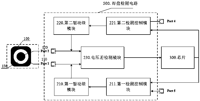
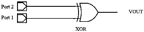
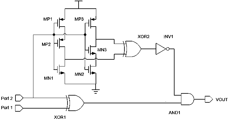
[0045] The present invention provides an embodiment of a ball planting state detection circuit for an isolated pad, referring to figure 1 As shown, it is provided with: an isolated pad 100, a pad detection circuit 200, a chip 300; an isolated pad 100, the isolated pad 100 includes a fi...


PUM


Abstract

The invention relates to the field of semiconductors, and discloses a detection circuit for the state of a planted ball of an isolated bonding pad. The detection circuit comprises the isolated bondingpad, a bonding pad detection circuit and a chip; the isolated bonding pad comprises a first conductive area, an insulated isolation area and a second conductive area; the first conductive area and the second conductive area are isolated by the insulted isolation area; the bonding pad detection circuit detects the state of the planted ball on the isolated bonding pad; the chip controls the bondingpad detection circuit to detect a voltage signal of the isolated bonding pad within set time, and acquires the state of the planted ball on the isolated bonding pad via the bonding pad detection circuit; the bonding pad detection circuit comprises a first driving stage module, a second driving stage module, a first detection control module, a second detection control module and a voltage difference detection module. According to the detection circuit provided by the invention, the programmable control on the working condition of the chip is achieved through detecting the state of the plantedball of the isolated bonding pad, the physical cost of the chip can be reduced, and the work flexibility of the chip can be increased.

Description

technical field [0001] The invention relates to the field of semiconductors, in particular to a ball planting state detection circuit for isolated pads. Background technique [0002] After the chip production is completed, it needs to be packaged before it can be applied to the actual product. The process of packaging is usually to connect the pads inside the chip with the pins of the package frame through wires. Traditionally used chip pads are usually only used to connect the inside of the chip to the package pins, and cannot provide more information. [0003] The applicant of the present invention proposed a new type of isolated pad in "An isolated pad and a chip containing the pad, patent application number: 201711289369.9". A complete pad is divided into the first The conductive area, the second conductive area and the insulating isolation area. When the pad is not planted with balls, the first conductive area and the second conductive area are separated by the insulat...

Claims


Application Information

Patent Timeline
Patent Type & Authority Patents(China)
IPC IPC(8): G01R31/28
CPCG01R31/2896
Inventor 张小龙
Owner 2PAI SEMICON CO LTD
Why Eureka
Try Eureka