A preparation method of a novel wifi intelligent control curved surface LED display device

A technology for display devices and LED lamps, applied in semiconductor devices, nanotechnology for materials and surface science, instruments, etc., can solve problems such as module interference problems that cannot be solved in time, slow development progress, poor luminous consistency, etc.

Active Publication Date: 2020-10-27
JIANGXI LIANCHUANG NANFEN TECHNOLOGY CO LTD
View PDF6 Cites 0 Cited by
  • Summary
  • Abstract
  • Description
  • Claims
  • Application Information

AI Technical Summary

Problems solved by technology

[0004] 1) The development progress is slow, the interference problem between modules cannot be solved in time, and there is a waste of PCB board resources;
[0005] 2) The traditional colorful display adopts LED mounting display of different colors. There is a voltage difference of about 1V between different color LEDs, and the cost of the driving circuit rises significantly; poor consistency;
[0006] 3) The luminous effect design of the traditional curved surface structure uses a segmented PCB board to ensure that the distance between the LED lamp beads and the luminous surface is consistent to achieve a uniform luminous effect. This method is difficult to process, and there is a connection reliability problem between the PCB boards.

Method used


Image

  • A preparation method of a novel wifi intelligent control curved surface LED display device
  • A preparation method of a novel wifi intelligent control curved surface LED display device
  • A preparation method of a novel wifi intelligent control curved surface LED display device

Examples


Embodiment Construction

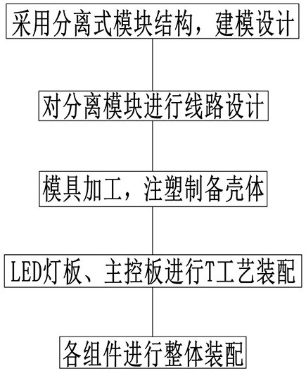
[0033] In order to make the object, technical solution and advantages of the present invention clearer, the present invention will be further described in detail below in conjunction with the accompanying drawings and embodiments. It should be understood that the specific embodiments described here are only used to explain the present invention, not to limit the present invention.

[0034] On the contrary, the invention covers any alternatives, modifications, equivalent methods and schemes within the spirit and scope of the invention as defined by the claims. Further, in order to make the public have a better understanding of the present invention, some specific details are described in detail in the detailed description of the present invention below. The present invention can be fully understood by those skilled in the art without the description of these detailed parts.

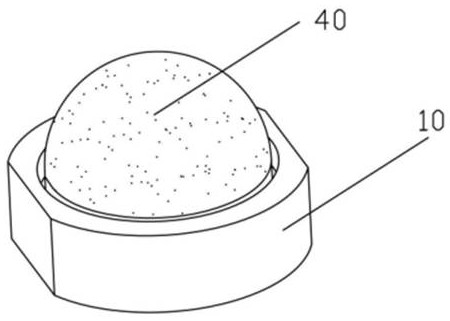
[0035] Such as figure 1 As shown, it is a schematic diagram of the overall structure of the first emb...


PUM


Abstract

The invention relates to the technical field of curved surface LEDs, and specifically relates to a preparation method of a novel WiFi intelligent control type curved surface LED display device. The preparation method comprises the following specific steps: S1, determining a project product to be of a separated module structure, and carrying out system structure design on an LED module; S2, carrying out circuit design on an infrared module, a WIFI module and an LED module; S3, after mold processing is completed, preparing a shell piece through an injection molding process; S4, carrying out SMTtechnology assembly on an LED lamp panel and a main control panel; and S5, researching and determining an assembly technology, and carrying out integral assembling on each component. A white LED lampbead is taken as a light source, multi-colored display is realized by printing different colors of printing inks on a diaphragm, and voltage difference among different colors of lamp beads is solved perfectly. A display module (integrated infrared module), a main control module and a WIFI module are separated, the interference among different signals during integration on the same PCB is reduced,and simultaneously, the exchange of each functional module is facilitated.

Description

technical field [0001] The invention relates to the technical field of curved LEDs, in particular to a method for preparing a novel WiFi smart-controlled curved LED display device. Background technique [0002] At present, the LED display modules used in conventional home appliances are composed of plastic casings, PCB boards, LED lamp beads, connecting wires, diaphragms, electronic components, etc., and can only simply indicate the status of home appliances when they are working. [0003] On the basis of the conventional LED display module, the client adds functions such as the main control module, infrared module and WIFI module. Related issues with this approach to development are: [0004] 1) The development progress is slow, the interference problem between modules cannot be solved in time, and there is a waste of PCB board resources; [0005] 2) The traditional colorful display adopts LED mounting display of different colors. There is a voltage difference of about 1V...

Claims


Application Information

Patent Timeline
Patent Type & Authority Patents(China)
IPC IPC(8): H01L33/58H01L33/60H01L33/44B82Y30/00G09F9/33
CPCB82Y30/00G09F9/33H01L33/44H01L33/58H01L33/60H01L2933/0025H01L2933/0058
Inventor 刘亮刘芳娇钟传根张帆杨爱兰涂俊清丁永华赵彦东李凝华肖章权
Owner JIANGXI LIANCHUANG NANFEN TECHNOLOGY CO LTD
Why Eureka
Try Eureka