A single particle sensitive gas sensor and its preparation method and application

A gas sensor and sensor technology, applied in the direction of instruments, scientific instruments, measuring devices, etc., can solve the problems of semiconductor material crystal structure damage, response recovery time as high as several to tens of minutes, complex operation, etc.

Active Publication Date: 2021-09-07
HUZHOU TEACHERS COLLEGE
View PDF14 Cites 0 Cited by
  • Summary
  • Abstract
  • Description
  • Claims
  • Application Information

AI Technical Summary

Problems solved by technology

Generally, semiconductor gas sensors often need to work at a higher temperature, but continuous high temperature work will destroy the crystal structure of the semiconductor material, resulting in unstable sensor performance.
[0003] At present, ultraviolet enhancement and inhibition of the growth of sensitive particles are common ways to improve the above problems. Among them, ultraviolet enhancement mainly uses ultraviolet light to excite sensitive materials instead of heating elements to thermally excite materials. This method can improve the room temperature gas-sensing properties of sensitive materials. and normal temperature conductivity; but its response recovery time is as high as several to tens of minutes, and the sensitivity is greatly reduced
At the same time, inhibiting the growth of a single sensitive particle is mainly achieved by preparing a hierarchical structure, but from the preparation of the hierarchical structure to the preparation of the sensor, operations such as spin coating or coating are required to form a sensitive material film layer, which is usually due to particles A dense film is formed by the aggregation of the sensor, which is not conducive to the improvement and stability of the gas sensing performance of the sensor
[0004] On the basis of the above, the existing technology solves the problem of the growth of a single sensitive particle by preparing a single nanoparticle to construct a gas sensor; in the process of preparing a single nanoparticle gas sensor, focused ion beam deposition is mainly used to achieve electrode deposition control, or by means of contact AFM is used to realize the control of sensitive materials, so as to realize the contact between sensitive materials and electrodes, but the equipment used in the method is more expensive and the operation is more complicated

Method used


Image

  • A single particle sensitive gas sensor and its preparation method and application
  • A single particle sensitive gas sensor and its preparation method and application
  • A single particle sensitive gas sensor and its preparation method and application

Examples


preparation example Construction

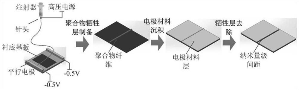
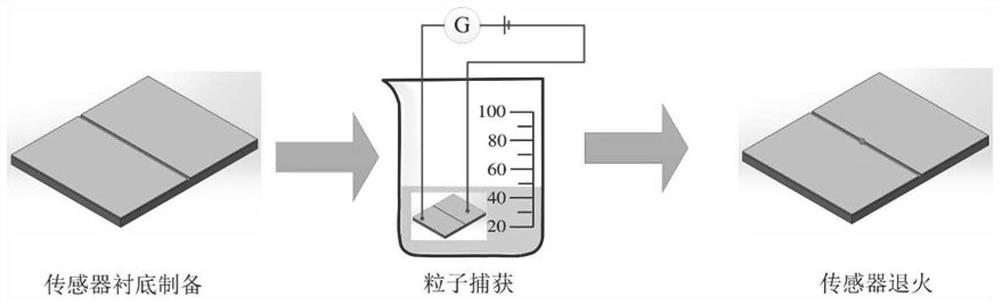
[0030] The invention provides a method for preparing a single particle sensitive gas sensor, comprising the following steps (such as figure 2 shown):

[0031] Provide the sensor substrate;

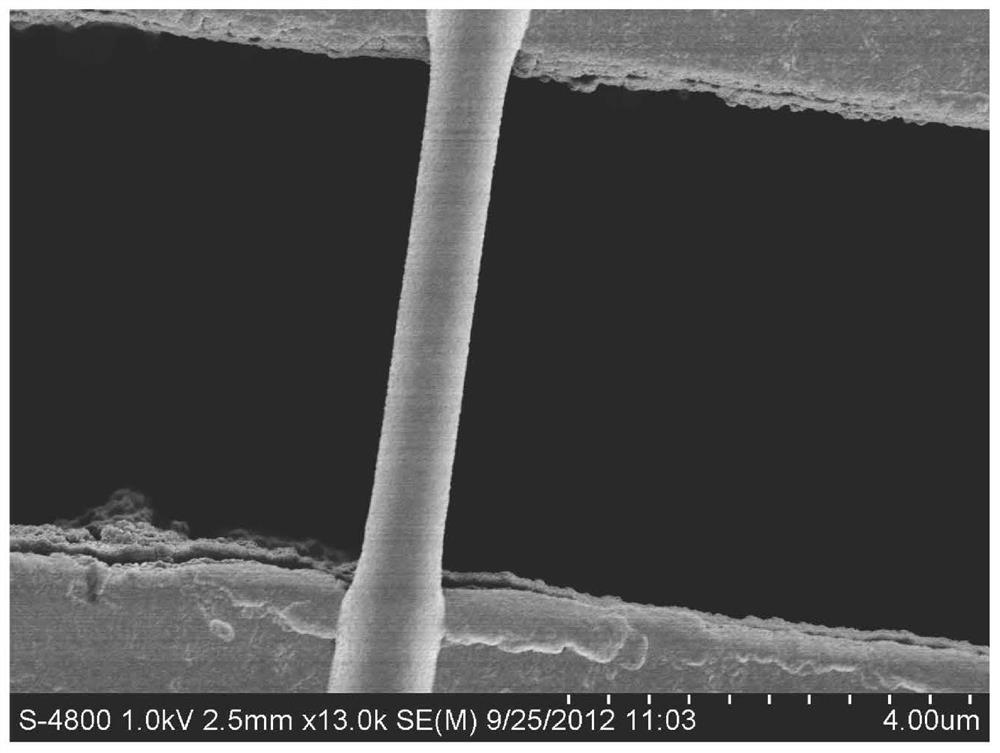
[0032] Depositing a single particle on the surface of the sensor substrate by a single particle capture method to form a single particle sensitive layer to obtain a single particle sensitive gas sensor precursor;

[0033] The single particle sensitive gas sensor precursor is annealed to obtain a single particle sensitive gas sensor.

[0034] In the present invention, unless otherwise specified, all raw materials are commercially available products well known to those skilled in the art.

[0035] The present invention provides a sensor substrate. In the present invention, the preparation method of the sensor substrate preferably includes the following steps:

[0036] After depositing the polymer fiber sacrificial layer and the electrode material layer sequentially on the sensor substra...

Embodiment 1

[0061] Mix 0.8 g of polyvinylpyrrolidone and 10 mL of ethanol, and stir in a magnetic stirrer until a uniform solution is formed to obtain an electrospinning solution;

[0062] The electrospinning solution was placed in a syringe, and an orderly arranged polyvinylpyrrolidone fiber sacrificial layer was deposited on the nitrided silicon wafer by an electric field-assisted ordered electrospinning method (conditions of the electric field-assisted ordered electrospinning method : the distance between the needle of the syringe and the silicon chip is 10cm, and the voltage is 11kV; the liquid supply flow rate of the syringe is 0.3mL / h; the parallel electrode voltage of the electric field is 0.5kV, and the distance between the parallel electrodes is 1cm);

[0063] Using magnetron sputtering to sequentially deposit the underlying metal tantalum (5nm in thickness) and gold (50nm in thickness) to form an electrode material layer;

[0064] Place the above-mentioned sensor substrate depos...

Embodiment 2

[0069] Mix 0.6 g of polyvinyl alcohol and 10 mL of ethanol, and stir in a magnetic stirrer until a uniform solution is formed to obtain an electrospinning solution;

[0070] The electrospinning solution was placed in a syringe, and an orderly arranged polyvinyl alcohol fiber sacrificial layer was deposited on the nitrided silicon wafer by an electric field-assisted ordered electrospinning method (conditions of the electric field-assisted ordered electrospinning method : the distance between the needle of the syringe and the silicon wafer is 13cm, and the voltage is 10.5kV; the liquid supply flow rate of the syringe is 0.2mL / h; the parallel electrode voltage of the electric field is -0.1kV, and the distance between the parallel electrodes is 0.5cm);

[0071] The underlying metal tantalum (thickness is 10nm) and platinum (thickness is 100nm) are sequentially deposited by magnetron sputtering;

[0072] Place the above-mentioned sensor substrate deposited with the polyvinyl alcoho...


PUM

PropertyMeasurementUnit
thicknessaaaaaaaaaa
thicknessaaaaaaaaaa
concentrationaaaaaaaaaa

Abstract

The present invention relates to the technical field of gas sensors, in particular to a single particle sensitive gas sensor and its preparation method and application. The preparation method of a single particle sensitive gas sensor provided by the present invention comprises the following steps: providing a sensor substrate; The particle capture method deposits single particles on the surface of the sensor substrate to obtain a single particle sensitive gas sensor precursor; the single particle sensitive gas sensor precursor is annealed to obtain a single particle sensitive gas sensor. The preparation method of the present invention is low in cost and simple in operation; the single particle sensitive gas sensor prepared by the preparation method can avoid particle aggregation and particle growth, thereby giving full play to the structural advantages of nanoparticles, increasing the specific surface area, improving Sensitivity, contribute to the response recovery rate of gas in the process of surface adsorption and desorption; it can also solve the instability problem caused by particle aggregation and secondary growth.

Description

technical field [0001] The invention relates to the technical field of gas sensors, in particular to a single particle sensitive gas sensor and its preparation method and application. Background technique [0002] Due to the characteristics of large specific surface area and rich surface defects, nanomaterials are widely used in gas sensors. Generally, semiconductor gas sensors need to work at a higher temperature, but continuous high temperature work will damage the crystal structure of the semiconductor material, resulting in unstable performance of the sensor. [0003] At present, ultraviolet enhancement and inhibition of the growth of sensitive particles are common ways to improve the above problems. Among them, ultraviolet enhancement mainly uses ultraviolet light to excite sensitive materials instead of heating elements to thermally excite materials. This method can improve the room temperature gas-sensing properties of sensitive materials. And normal temperature cond...

Claims


Application Information

Patent Timeline
Patent Type & Authority Patents(China)
IPC IPC(8): G01N27/00
CPCG01N27/00
Inventor 范祥祥徐亚娟贺无名黄旭曾梦佳
Owner HUZHOU TEACHERS COLLEGE
Why Eureka
Try Eureka