Semiconductor device having protection circuit

A technology for overall protection and circuit protection, which is applied in the manufacture of semiconductor devices, electrical solid state devices, semiconductor/solid state devices, etc., and can solve problems such as inability to effectively protect circuits

Inactive Publication Date: 2003-01-22
RENESAS ELECTRONICS CORP
View PDF0 Cites 0 Cited by
  • Summary
  • Abstract
  • Description
  • Claims
  • Application Information

AI Technical Summary

Problems solved by technology

[0019] According to the above point of view, the conventional protection circuit cannot effectively protect the circuit from damage caused by excessive voltage

Method used


Image

  • Semiconductor device having protection circuit
  • Semiconductor device having protection circuit
  • Semiconductor device having protection circuit

Examples


Embodiment Construction

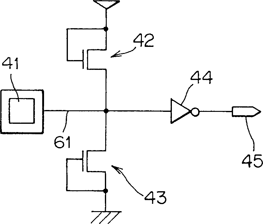
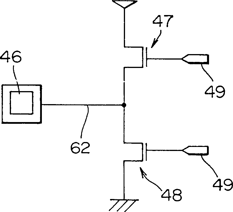
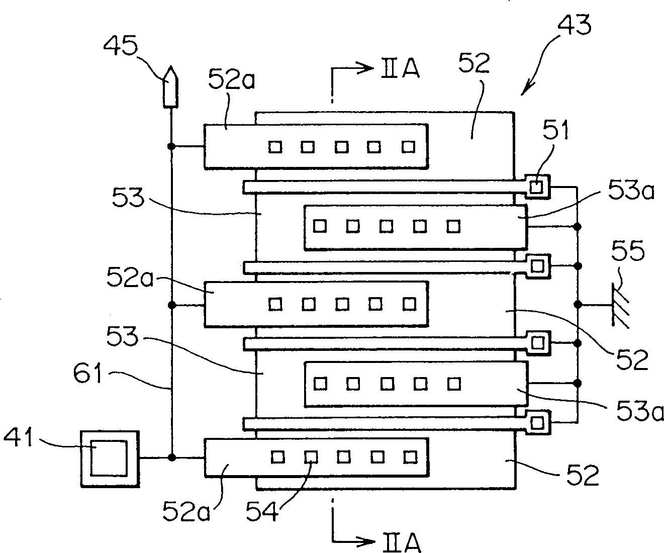
[0035] DETAILED DESCRIPTION OF THE PREFERRED EMBODIMENTS Preferred embodiments of the present invention will be described in detail with reference to the accompanying drawings. Figure 5A In order to draw a typical diagram of the input protection circuit of the semiconductor device of the first embodiment of the present invention, and Figure 5B Then, it is a typical diagram showing the output protection circuit of the semiconductor device of the first embodiment. Such as Figure 5A As shown in , the gate electrode 15 comprises a strip-shaped conductive film formed on a semiconductor substrate (not shown). This gate electrode 15 exhibits a zigzag wavy shape having alternating crests and troughs in a plan view of the semiconductor substrate. A drain diffusion layer 14 is formed in one of the two diffusion regions on the surface of the semiconductor substrate defined by the gate electrode 15, and a source diffusion layer 16 is formed in the other region. That is, one region s...


PUM


Abstract

Protection circuits for preventing an internal circuit on a semiconductor substrate from destroying due to an excess voltage are formed on the output end and input end of an internal circuit. The protection circuit on the input end has a gate electrode comprised of a band-like conductive film. This gate electrode is grounded and has a shape zigzagging in a waveform with crests and troughs alternately appearing in a planar view. A drain diffusion layer connected to an output end of the internal circuit is formed in one of two diffusion regions of the surface of the semiconductor substrate that are defined by the gate electrode, and a source diffusion layer grounded is formed in the other region. The source diffusion layer and the drain diffusion layer are formed integral with each other, so that the protection circuit on the input end is substantially constituted of one buffer transistor.

Description

technical field [0001] The present invention relates to a semiconductor device with a protection circuit for preventing internal circuits from being destroyed due to overvoltage, more particularly, to a semiconductor device with an integral protection circuit capable of improving withstand voltage protection. Background technique [0002] An input protection circuit and an output protection circuit are respectively provided at the input end and the output end of the internal circuit in the semiconductor device to prevent the internal circuit from being destroyed due to excessive voltage. In recent years, by Thomson L. Paul Green et al. in February 1992, the American Institute of Electrical Engineers Electronic Devices Volume 39, No. 2, 382-384 pages "By ensuring uniform current to improve the silicide n-MOS The article “Electric Spark Failure (ESD) Threshold Voltage of Output Transistors” proposes to design higher integration and higher density semiconductor devices by shrin...

Claims


Application Information

Patent Timeline
IPC IPC(8): H01L27/04H01L21/822H01L21/8234H01L23/62H01L27/02H01L27/088H01L29/78
CPCH01L27/0277H01L27/04
Inventor 入野仁
Owner RENESAS ELECTRONICS CORP
Why Eureka
Try Eureka