Flexible circuit board, capacitive screen and processing method of flexible circuit board
A flexible circuit board and conductive sheet technology, applied in printed circuit components, electrical digital data processing, and electrical connection of printed components, etc., can solve problems such as poor contact of flexible circuit boards, and achieve the purpose of avoiding poor contact, simple processing technology, and electrical conductivity. good performance
- Summary
- Abstract
- Description
- Claims
- Application Information
AI Technical Summary
Problems solved by technology
Method used
Image
Examples
Embodiment 1
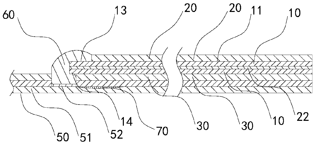
[0064] Such as Figure 1 to Figure 7 As shown, the capacitive screen 50 includes a screen body 51 and a flexible circuit board.
[0065] The flexible circuit board includes: a base layer 22, a conductive layer 10 and a protective layer. The conductive layer 10 is attached to the base layer 22. The protective layer covers the conductive layer 10. The conductive layer 10 has a conductive sheet 11 and a conductive wire 12. The conductive sheet 11 and the conductive wire 12 are electrically connected to each other, the conductive sheet 11 is located at the conductive connection side, and the conductive sheet 11 has a first relief gap 16, and the opening width of the first relief gap 16 gradually decreases from the outside to the inside (this embodiment In an example, the edge of the first abdication 16 is an arc segment).
[0066] There are conductive contacts 52 on the screen body 51, and the back surface of the flexible circuit board is electrically connected to the screen body...
Embodiment 2
[0094] Such as Figure 8 As shown, compared with the first embodiment, this embodiment has the first relief gap 16 whose edge is an arc segment, and there is only one arc segment.
[0095] This embodiment has the following advantages:
[0096] In this embodiment, when processing the conductive sheet 11 , the drill only needs to drill one cut and drill an arc segment to complete the processing of the conductive sheet 11 , and the process of processing the conductive sheet 11 is more convenient.
PUM
| Property | Measurement | Unit |
|---|---|---|
| Width | aaaaa | aaaaa |
| Width | aaaaa | aaaaa |
| Width | aaaaa | aaaaa |
Abstract
Description
Claims
Application Information
 - R&D Engineer
- R&D Manager
- IP Professional
- Industry Leading Data Capabilities
- Powerful AI technology
- Patent DNA Extraction
Browse by: Latest US Patents, China's latest patents, Technical Efficacy Thesaurus, Application Domain, Technology Topic, Popular Technical Reports.
© 2024 PatSnap. All rights reserved.Legal|Privacy policy|Modern Slavery Act Transparency Statement|Sitemap|About US| Contact US: help@patsnap.com


