
Eureka
For R&D, Eureka makes reading and utilizing patents & technical documents easy.
Eureka AIR
Designed for self-driven R&D workflows. Generate viable solutions, solve complex R&D challenges, empower your innovation with AI.

Eureka Materials
Designed for material experts only. Revolutionize your material R&D, from search, analyze, to developing new materials.

TechResearch
Generate reliable direction feasibility study reports for your R&D in just a few steps.

TechSeek
Discover and master advanced knowledge NOW. Basics, ideas, possibilities, all at once.

TechMind
As an expert in R&D Theories, TechMind can generates customized viable solutions instantly.

TechRisk
Analyze your overall solution with one click, know your potential R&D risks in advance.

TechMonitor
Get weekly tech updates, stay abreast of the latest tech innovations and key insights.
Patterning device and patterning method
A patterned, hollow area technology, applied in decorative arts, special decorative structures, processes for producing decorative surface effects, etc., can solve the problem of uneven diffusion of liquid optical glue
- Summary
- Abstract
- Description
- Claims
- Application Information
AI Technical Summary
Problems solved by technology
Method used
Image


Examples
Embodiment Construction
[0042] In order to make the description of this disclosure more detailed and complete, reference may be made to the attached drawings and various implementations described below. Elements in the drawings are not drawn to scale and are provided merely to illustrate the present disclosure. Numerous practical details are described below in order to provide a thorough understanding of the present disclosure, however, those of ordinary skill in the relevant art will understand that the present disclosure can be practiced without one or more of the practical details, and thus, these details are not apply to define this disclosure.
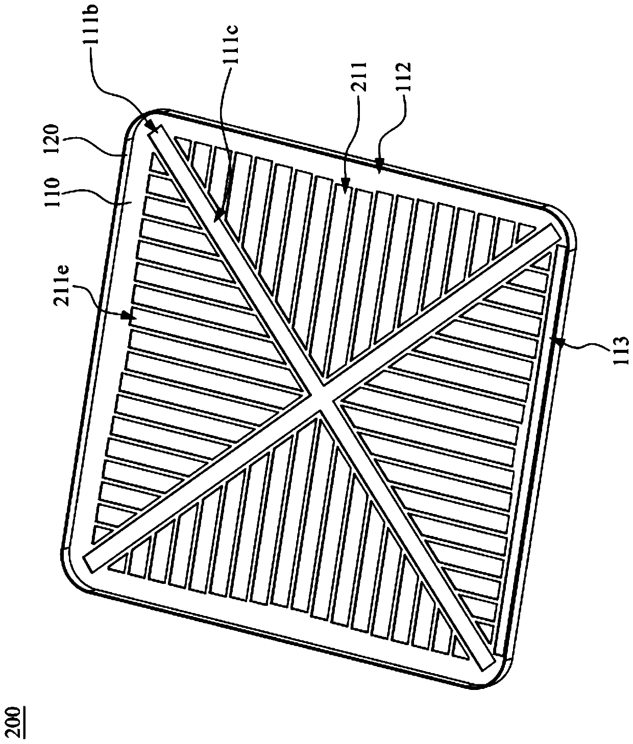
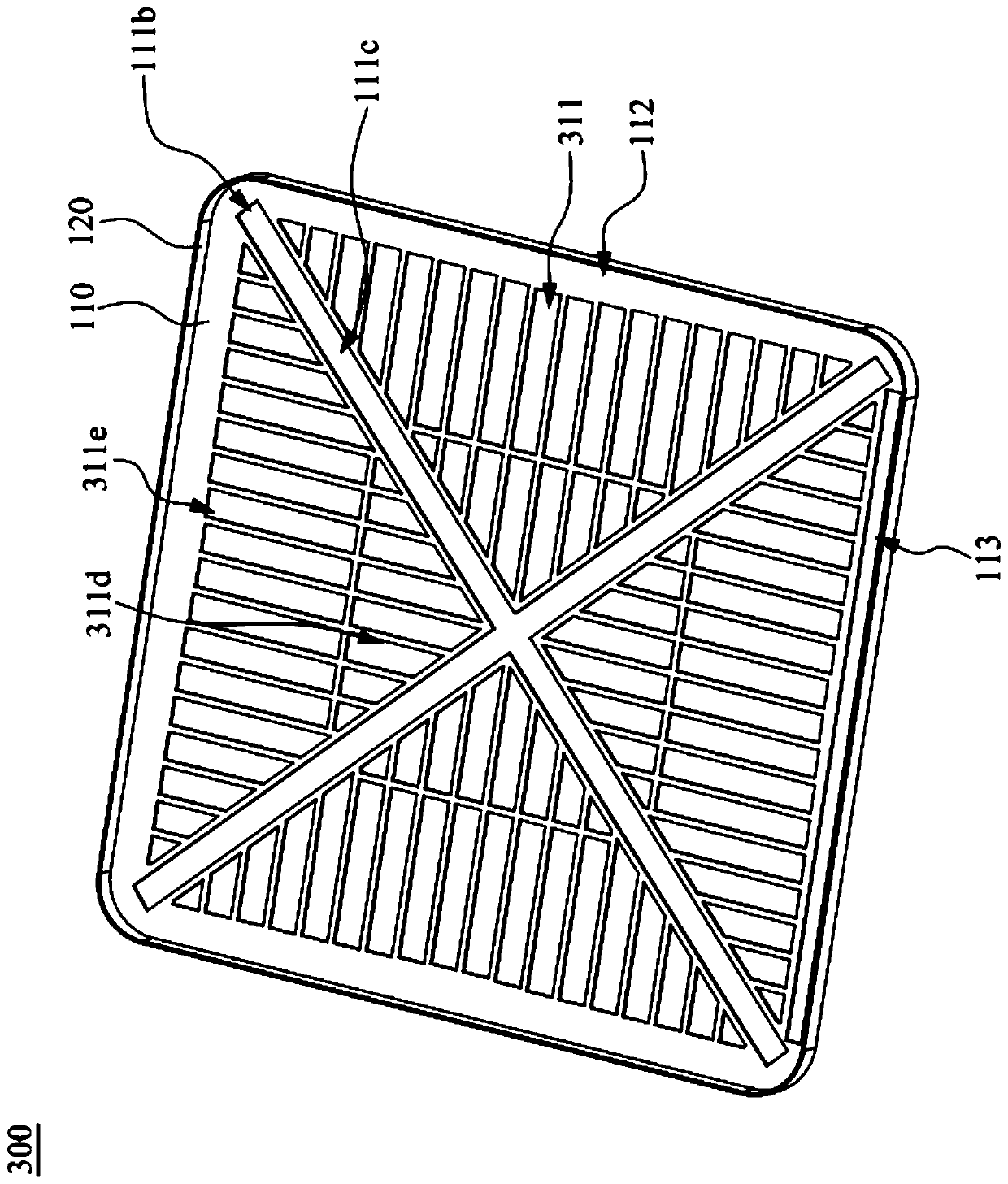
[0043] Please refer to figure 1 , which is a perspective view illustrating a patterning device 100 according to an embodiment of the present disclosure. The patterning device 100 is applied to bonding of display devices, and it can be used for substrates to be bonded (such as cover glass, not shown in figure 1 Middle) to form a specific liquid optical...
PUM
 Abstract
Description
Claims
Application Information
 - R&D Engineer
- R&D Manager
- IP Professional
- Industry Leading Data Capabilities
- Powerful AI technology
- Patent DNA Extraction
Browse by: Latest US Patents, China's latest patents, Technical Efficacy Thesaurus, Application Domain, Technology Topic, Popular Technical Reports.
© 2024 PatSnap. All rights reserved.Legal|Privacy policy|Modern Slavery Act Transparency Statement|Sitemap|About US| Contact US: help@patsnap.com