
Display device using semiconductor light-emitting element

A technology for display devices and light-emitting elements, which is applied in the direction of semiconductor devices, electric solid-state devices, and light-emitting materials, and can solve problems such as brightness reduction, and achieve the effects of ensuring structural reliability, improving display efficiency and color purity, and improving color purity

Active Publication Date: 2019-04-26
LG ELECTRONICS INC
View PDF13 Cites 4 Cited by
  • Summary
  • Abstract
  • Description
  • Claims
  • Application Information

AI Technical Summary

Problems solved by technology

In this structure, the yellow phosphor has a peak wavelength of 500 to 600 nanometers, and therefore, there is a problem that the brightness of red with a wavelength of more than 600 nanometers decreases

Method used


Image

  • Display device using semiconductor light-emitting element
  • Display device using semiconductor light-emitting element
  • Display device using semiconductor light-emitting element

Examples


Embodiment Construction

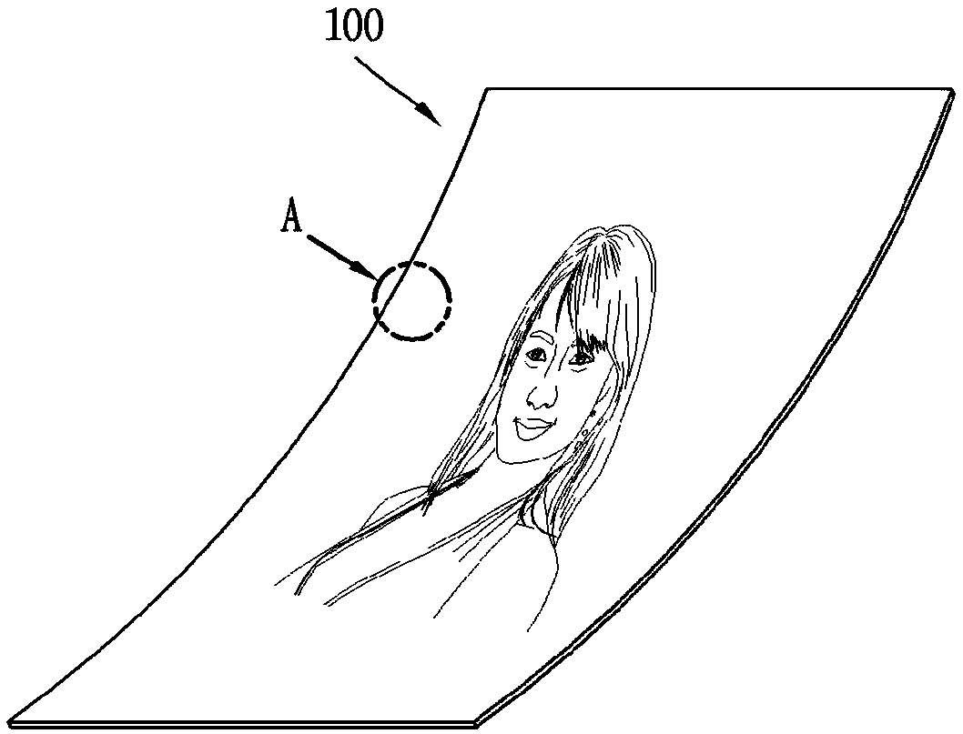
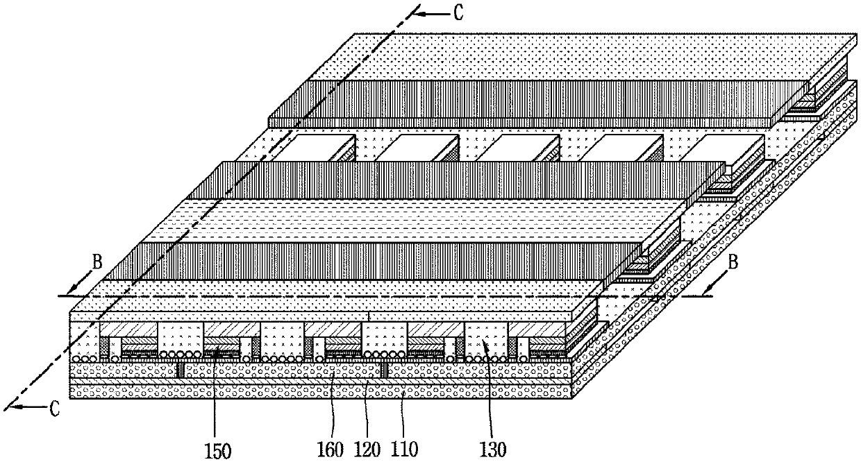
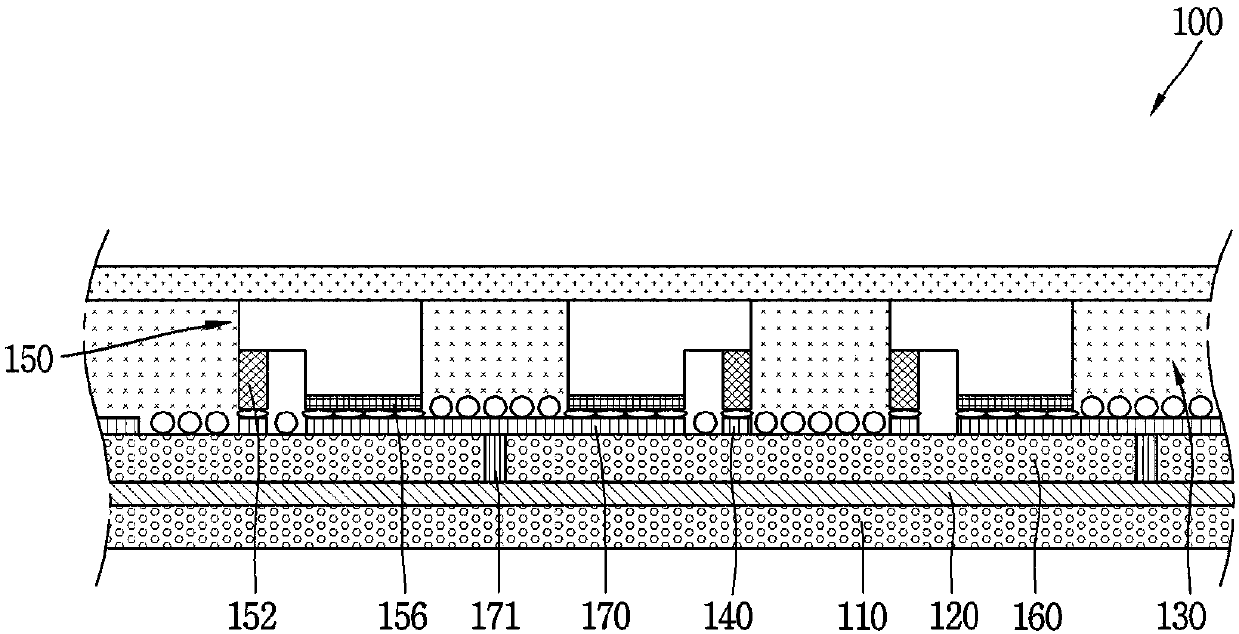
[0037] Hereinafter, embodiments disclosed herein will be described in detail with reference to the accompanying drawings, and the same or similar elements will be designated with the same reference numerals regardless of the reference numerals in the drawings, and redundant descriptions thereof will be omitted. The suffixes "module" and "unit" used for constituent elements disclosed in the following description are intended only for simple description of the specification, and the suffixes themselves do not give any special meaning or function. In describing the present disclosure, if a detailed explanation for a related known function or construction is considered to unnecessarily divert the gist of the present disclosure, such explanation has been omitted but will be understood by those skilled in the art. Also, it should be noted that the accompanying drawings are only for illustration to easily explain the concept of the present invention, and thus, they should not be const...


PUM

PropertyMeasurementUnit
thicknessaaaaaaaaaa

Abstract

The present invention relates to a display device and, particularly, to a display device using a semiconductor light-emitting element. The display device according to the present invention comprises:a substrate having a wiring electrode; a plurality of semiconductor light-emitting elements electrically connected to the wiring electrode; a plurality of fluorescent substance layers for converting awavelength of light; a wavelength conversion layer having a plurality of partitioning parts formed between the plurality of fluorescent substance layers, and disposed so as to cover the plurality ofsemiconductor light-emitting elements; and a color filter disposed so as to cover the wavelength conversion layer, wherein at least one of the plurality of fluorescent substance layers has a pluralityof layers.

Description

technical field [0001] The present disclosure relates to display devices, and more particularly, to display devices using semiconductor light emitting elements. Background technique [0002] In recent years, display devices having excellent characteristics such as low profile, flexibility, etc. have been developed in the field of display technology. In contrast, currently commercialized primary displays are represented by liquid crystal displays (LCDs) and active matrix organic light emitting diodes (AMOLEDs). However, there are problems such as poor response time, difficulty in achieving flexibility in the case of LCD, and disadvantages such as short lifetime, poor yield, and low flexibility in the case of AMOLED. [0003] On the other hand, light-emitting diodes (LEDs) are well-known light-emitting elements for converting electric current into light, and have been used since red LEDs using GaAsP compound semiconductors were manufactured on the market together with GaP:N-b...

Claims


Application Information

Patent Timeline
Patent Type & Authority Applications(China)
IPC IPC(8): H05B33/12H05B33/10H01L33/50H01L33/58H01L33/00
CPCH01L33/00H01L33/50H01L33/58H05B33/14H05B33/12H05B33/10H01L33/504H01L33/005H01L2924/12041H01L2933/0041C09K11/7706H01L25/0753H01L33/60
Inventor 崔桓准李勇翰
Owner LG ELECTRONICS INC
Learn More