
Display panel

A display panel and display area technology, applied in the direction of instruments, electrical digital data processing, electrical components, etc., can solve the problems of metal residue, metal residue in difficult post-metal manufacturing process, and defective panels, so as to improve the yield rate and avoid the risk of short circuit Effect

Inactive Publication Date: 2019-04-02
WUHAN CHINA STAR OPTOELECTRONICS SEMICON DISPLAY TECH CO LTD
View PDF5 Cites 5 Cited by
  • Summary
  • Abstract
  • Description
  • Claims
  • Application Information

AI Technical Summary

Problems solved by technology

[0005] The present invention provides a display panel to solve the problem of the existing display panel. Since the inorganic layer and the organic layer at the cutting line will be removed, the inorganic layer is generally thin, and it is not easy to cause metal residue in the post-metal process at the cutting line. The thickness of the organic layer is relatively thick, and the metal residue in the post-metal process is easy to occur on the cutting edge of the organic layer, which causes short circuits between the signal terminals of the panel and short circuits of different signals, which in turn leads to poor technical problems of the panel

Method used


Image

  • Display panel
  • Display panel
  • Display panel

Examples


Embodiment 1

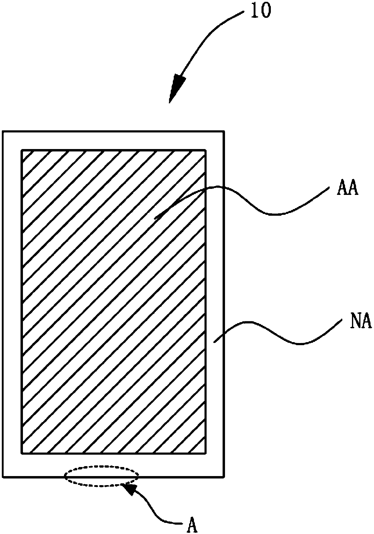
[0031] like figure 2 As shown, this embodiment provides a display panel 10, which defines a display area AA and a non-display area NA disposed outside the display area AA, and the non-display area NA in this embodiment surrounds the display area AA is set, the display area AA is used to display images, and the non-display area NA is used to accommodate signal wiring and other components that block light.

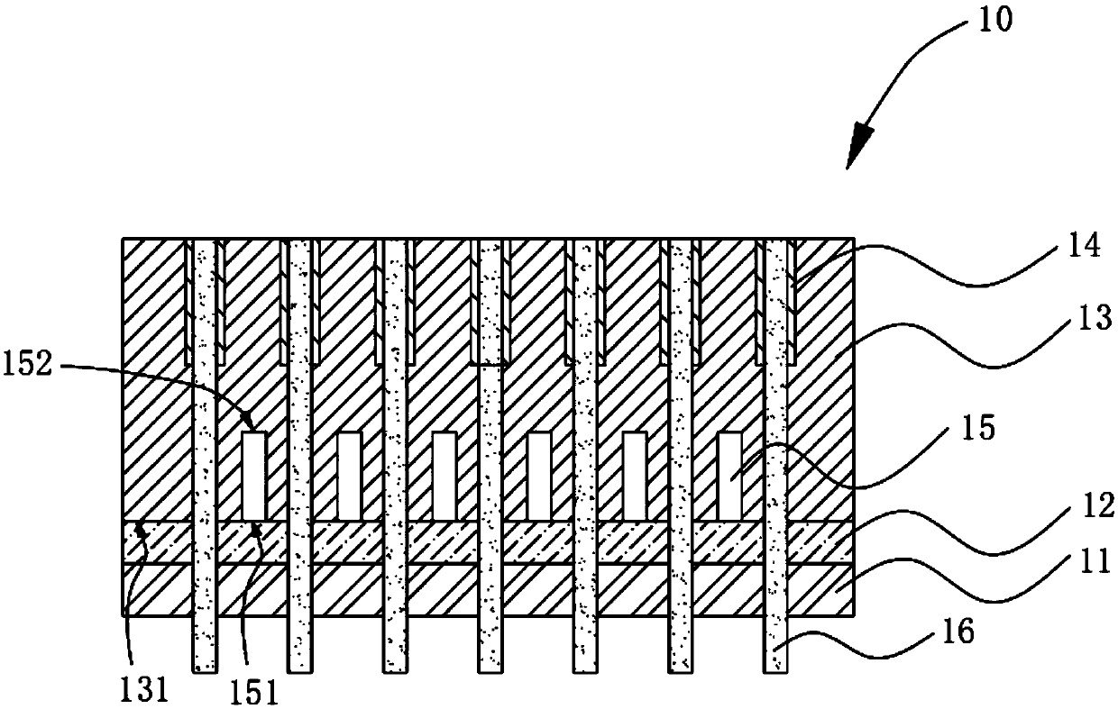
[0032] like image 3 as shown, image 3 for figure 2 Schematic diagram of the enlarged structure at A in, image 3 In a top view, the display panel 10 includes a base substrate 11 , an inorganic layer 12 , an organic layer 13 , a plurality of binding terminals 14 , and a plurality of signal terminals 16 .

[0033] Wherein, the inorganic layer 12 is disposed on the base substrate 11 , the organic layer is disposed on the inorganic layer 12 , and a plurality of binding terminals 14 are disposed on the organic layer 13 in parallel.

[0034] The organic layer 13 is provid...

Embodiment 2

[0049] like Figure 5 As shown, the display panel 20 includes a base substrate 21, an inorganic layer 22, an organic layer 23, a plurality of binding terminals 24, and a plurality of signal terminals (not shown in the figure).

[0050] A plurality of grooves 25 are opened on the organic layer 23 , and the grooves have opposite first sides 251 and second sides 252 .

[0051] Different from the first embodiment, the length of the groove 25 is different, and the second side 252 of the groove 25 is flush with the side of the binding terminal 24 close to the display area.

[0052] Other structures are the same as those in Embodiment 1, and will not be repeated here.

Embodiment 3

[0054] Please refer to Image 6 and Figure 7 The display panel 30 includes a base substrate 31, an inorganic layer 32, an organic layer 33, a plurality of binding terminals 34, and a plurality of signal terminals 36 (not shown in the figure), and the organic layer 33 has multiple Groove 35

[0055] The grooves 35 in this embodiment adopt a thinner and more design, so that the residual metal 37 in the post-metal process forms more discontinuous small pieces of metal, further reducing the risk of short circuit.


PUM


Abstract

A display panel is defined with a display region and a non-display region, wherein the non-display region is arranged outside the display region, the display panel comprises a substrate, a plurality of bonding terminals and an organic layer, wherein the bonding terminals are arranged on the substrate at intervals and are arranged at the non-display region, an organic layer is arranged on the substrate and comprises a first boundary, the first boundary is arranged at the non-display region and is arranged at outer sides of the bonding terminals, a plurality of parallel grooves are formed in theorganic layer along the first boundary, and at least one groove is formed between two adjacent bonding terminals. The display panel has the beneficial effects that the plurality of grooves are formedin an edge, near to a cutting way, of the organic layer, so that residual metal generated by the subsequent metal process is non-continuous, the panel short-circuit risk is effectively prevented, andthe yield of the panel is further improved.

Description

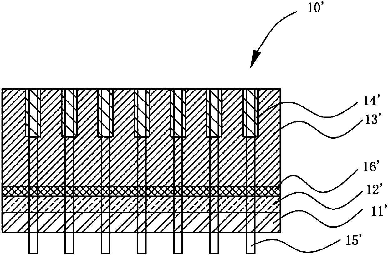
technical field [0001] The present invention relates to the field of display technology, in particular to a display panel. Background technique [0002] In the existing flexible panel design, the inorganic layer and the organic layer at the cutting line of the panel are generally removed to ensure the cutting quality and facilitate the subsequent splitting process. The inorganic layer and organic layer will remain outside the cutting line to protect the panel. Generally, the inorganic layer is thin, and the edge is not easy to cause metal residue, while the thickness of the organic layer is relatively thick. After the organic layer at the dicing line is removed, metal residue in the post-processing process is easy to occur at the edge of the organic layer and the scribing line. [0003] like figure 1 as shown, figure 1 It is a top view of the edge of the existing display panel with metal residues, the display panel includes a base substrate 11', an inorganic layer 12', an...

Claims


Application Information

Patent Timeline
Patent Type & Authority Applications(China)
IPC IPC(8): H01L27/12
CPCH01L27/1244G06F1/1637G06F1/1601G06F2200/1612G06F1/181G06F1/189
Inventor 张筱霞
Owner WUHAN CHINA STAR OPTOELECTRONICS SEMICON DISPLAY TECH CO LTD
Learn More