Feeding system applicable to super-large scale atomic layer deposition

An atomic layer deposition and feeding system technology, applied in the field of photovoltaic cell manufacturing and semiconductor manufacturing, can solve the problems of increasing the heating time of the product, the self-weight of the material chamber, and the lack of a uniform flow device in the intake air, so as to shorten the heating time and structure. Simple, uniform effect

Active Publication Date: 2019-03-29
南京爱通智能科技有限公司
View PDF10 Cites 2 Cited by
  • Summary
  • Abstract
  • Description
  • Claims
  • Application Information

AI Technical Summary

Problems solved by technology

This structure has the following disadvantages: the weight of the material chamber is very large, which is not conducive to transshipment; the large mass and heat capacity are also large, which is not conducive to heat utilization and increases the heating time of the product; it is inconvenient to load and unload the material at the top; Loading and unloading; there is no uniform flow device in the air intake, which is easy to generate dust

Method used


Image

  • Feeding system applicable to super-large scale atomic layer deposition
  • Feeding system applicable to super-large scale atomic layer deposition
  • Feeding system applicable to super-large scale atomic layer deposition

Examples


Embodiment

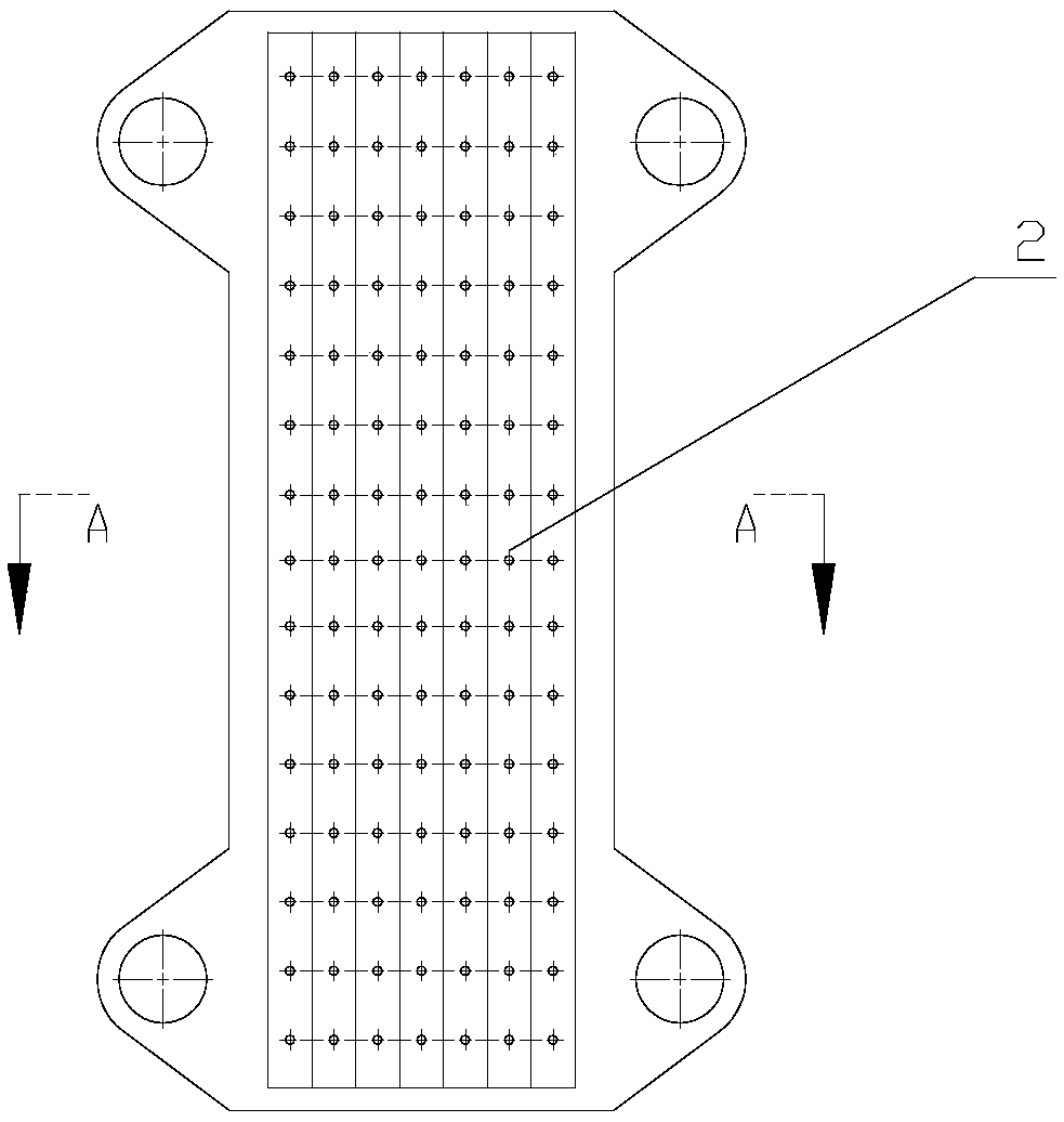
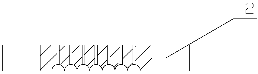
[0021] Embodiment: A feeding system suitable for ultra-large-scale atomic layer deposition, including a silicon wafer carrier 1 and a first end cap flange 2 and a second end cap method for clamping the silicon wafer carrier 1.

[0022] The silicon wafer carrier 1 includes several groups of carrier groups arranged side by side. Each carrier group is composed of multiple carriers. The carrier includes a carrier frame surrounded by two bottom plates and two side plates. The bottom plate and side plates of each carrier are connected end to end to form a hollow columnar structure; on the opposite sides of each carrier, there are several tooth slots evenly distributed from top to bottom on the opposite sides of each carrier. One correspondence, and the corresponding two teeth are located on the same plane, the corresponding two grooves on the two side plates carry two wafers, and the side of the two wafers to be coated faces outward, and the other side is attached to each other; Two wa...


PUM


Abstract

The invention discloses a feeding system applicable to super-large scale atomic layer deposition. The system comprises a silicon carrier and a first end cover flange and a second end cover flange which clamp the silicon carrier; the first end cover flange and the second end cover flange are connected into a whole through multiple shafts vertically penetrating through the first end cover flange andthe second end cover flange, and one ends of the shafts penetrate through the first end cover flange and are connected with the second end cover flange; the other ends of the shafts stretch out of the first end cover flange, a spring sleeves an extension part, shaft caps are arranged at the ends of protruding ends, and springs are limited at the protruding ends of the shafts. Accordingly, the silicon carrier serves as one part of an inner cavity, the deal load is greatly reduced, and transfer is light; meanwhile, the feeding system is heated directly, the heating rate can be obviously increased, the heating time is shortened, and the heat utilization rate is high.

Description

Technical field [0001] The present invention belongs to the field of semiconductor manufacturing, and specifically relates to the field of photovoltaic cell manufacturing. The atomic layer deposition (ALD) technology is applied to the photovoltaic field to produce equipment for ultra-large-scale products. Background technique [0002] With the scale of the photovoltaic industry and the rapid development of photovoltaic technology, ALD technology, that is, atomic layer deposition technology, has become an effective way to reduce costs and increase efficiency of photovoltaic products. The atomic layer deposition technology is to expose the product to two or more precursor gases for coating. The usual ALD equipment separates the coating chamber into a material chamber (inner chamber) and a vacuum chamber (outer chamber). The material chamber can be separated from the main equipment for loading. After the product is loaded, the material chamber can be transported to the vacuum chambe...

Claims


Application Information

Patent Timeline
Patent Type & Authority Applications(China)
IPC IPC(8): C23C16/455
CPCC23C16/45544Y02P70/50
Inventor 董仲
Owner 南京爱通智能科技有限公司
Why Eureka
Try Eureka