A scalable processing board based on high-speed and high-density connectors
A high-density connector and extended processing technology, applied in the field of scalable processing boards, can solve problems such as lack of extrusion resistance, easy damage, and easy heating of processing boards, so as to reduce development costs, increase use time, and shorten development cycles. Effect
- Summary
- Abstract
- Description
- Claims
- Application Information
AI Technical Summary
Problems solved by technology
Method used
Image
Examples
Embodiment Construction
[0036] The technical solutions of the present invention will be clearly and completely described below in conjunction with the embodiments. Apparently, the described embodiments are only some of the embodiments of the present invention, not all of them. Based on the embodiments of the present invention, all other embodiments obtained by persons of ordinary skill in the art without creative efforts fall within the protection scope of the present invention.
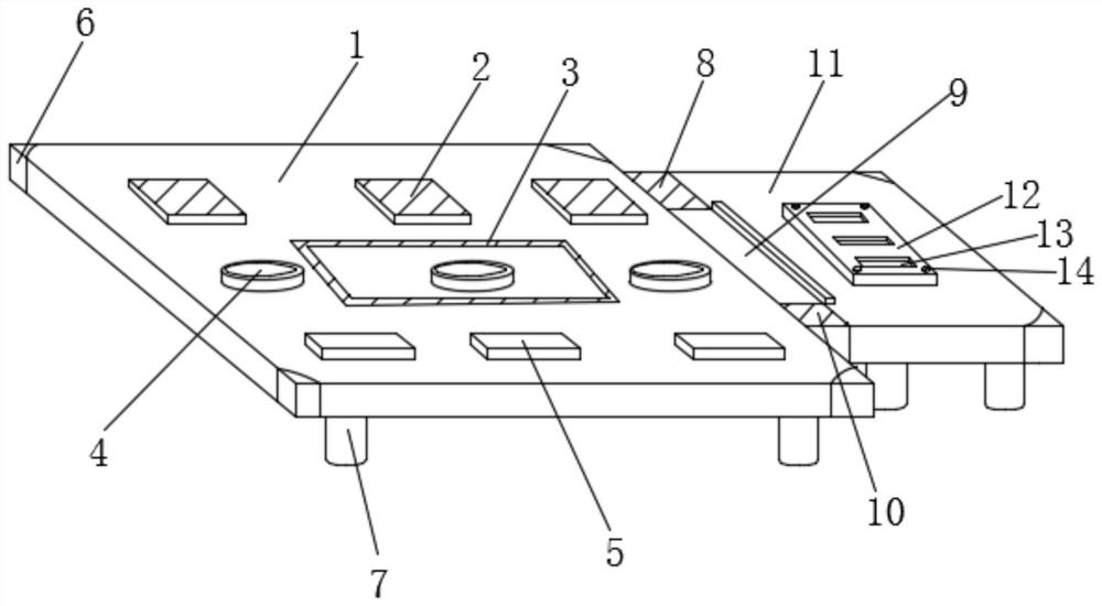
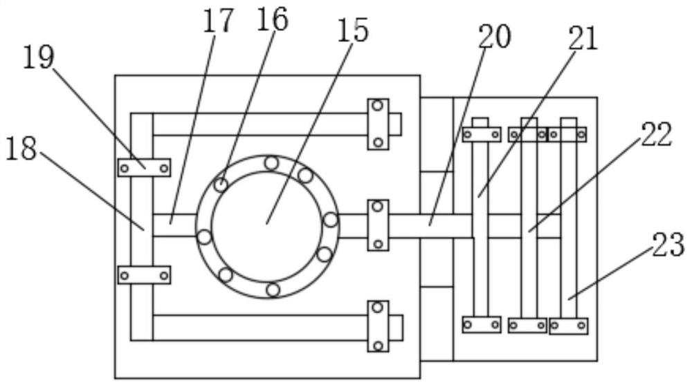
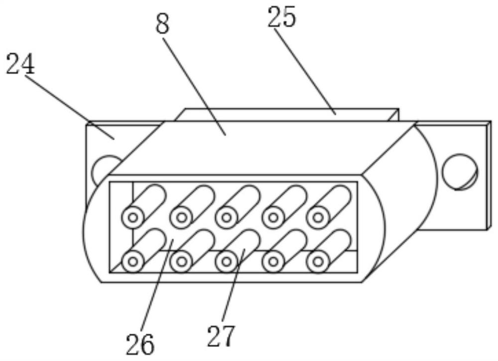
[0037] see Figure 1-8 As shown, a scalable processing board based on a high-speed high-density connector includes a sub-board 1 and a carrier board 11, and the upper surface of the sub-board 1 is equipped with a PPC chip 2, a DSP chip 4 and an FPGA 5, and the PPC chip 2 and the DSP chip 4 and FPGA5 are respectively arranged in parallel, and PPC chip 2, DSP chip 4 and FPGA5 are all provided with three groups, the middle part of the upper end surface of sub-board 1 is provided with wiring groove 3, four corners of sub-board ...
PUM
 Abstract
Description
Claims
Application Information
 - Generate Ideas
- Intellectual Property
- Life Sciences
- Materials
- Tech Scout
- Unparalleled Data Quality
- Higher Quality Content
- 60% Fewer Hallucinations
Browse by: Latest US Patents, China's latest patents, Technical Efficacy Thesaurus, Application Domain, Technology Topic, Popular Technical Reports.
© 2025 PatSnap. All rights reserved.Legal|Privacy policy|Modern Slavery Act Transparency Statement|Sitemap|About US| Contact US: help@patsnap.com


