Method for detecting defects in and on film

A detection method and internal defect technology, which is applied in the field of optical detection, can solve the problems of film defects on the film and the inability to distinguish the defects in the film or on the film, so as to improve the detection rate, reduce network traffic and storage space, and increase production capacity. Effect

Inactive Publication Date: 2019-02-26
SUZHOU JINGLAI OPTO CO LTD
View PDF7 Cites 4 Cited by
  • Summary
  • Abstract
  • Description
  • Claims
  • Application Information

AI Technical Summary

Problems solved by technology

[0003] The purpose of the present invention is to solve the problem that the detection method of the prior art mentioned in the above background technology cannot distinguish between defects in the film or on the film, and provide a method for detecting defects in the film on the film

Method used


Image

  • Method for detecting defects in and on film
  • Method for detecting defects in and on film
  • Method for detecting defects in and on film

Examples


Embodiment Construction

[0028] The present invention will be further described in detail below in conjunction with the drawings and specific embodiments.

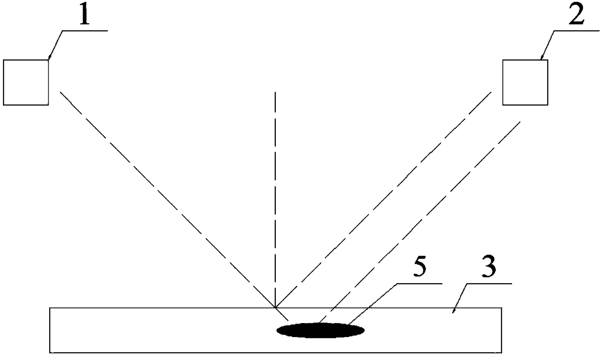
[0029] The schematic diagram of this embodiment is as Figure 1~3 As shown, the image capture unit 1 and the defect scanning unit 2 are used to capture images of the substrate to be tested on which the transparent film 3 is deposited, and then through data analysis of the captured image information, the defect is determined by the analysis results (this embodiment considers transparent There are some defective parts on the film 3, the defective parts are independent individuals, and the adjacent defective parts are distributed at intervals). Are the defects 4 on the transparent film 3 or the internal defects 5 located in the transparent film 3? This embodiment is to be tested The substrate is a flexible substrate or a glass substrate. The image capturing unit 1 of this embodiment is a high-precision optical camera, and the defect scanning unit 2 is ...


PUM


Abstract

The invention relates to the technical field of optical detection and particularly relates to a method for detecting defects in and on a film. A defect scanning unit is driven to scan a transparent substrate to be tested to acquire a defect portion of the substrate to be tested, the maximum or minimum gray level value of the defect portion is compared with a first standard value, and through comparison between the difference and the preset value, it is judged whether the defect portion is located in the film or on the film. According to the basic principle that the refractive indexes of the substrate to be tested and air are different, the defect in the film or on the film produces different gray-scale images on the taken image and through comparison, the defects in the film or on the filmare ensured so that detection efficiency of the defect portion is improved, a large amount of time is saved and the method has a great promotion value.

Description

Technical field [0001] The invention relates to the technical field of optical inspection, in particular to a method for detecting defects in the film on the film. Background technique [0002] The automatic optical inspection machine plays an important blocking inspection function in the panel (TFT / AMOLED) manufacturing process. However, as the panel size becomes larger and larger, the inspection resolution becomes higher and higher, and the number of relative defects is also increasing. In fact, not every type of defect will affect the next process. If all the detected defects are dealt with, it will undoubtedly greatly increase the man-hours of the inspection process and reduce the efficiency of panel inspection. For example, in the PI and LLO process of flexible board inspection, it is only necessary to detect defects on or in the film, and then adjust according to these defects. For example, in a certain process, only defects in the film will affect it, and defects on the fi...

Claims


Application Information

Patent Timeline
IPC IPC(8): G01N21/958
CPCG01N21/8851G01N21/958G01N2021/8887
Inventor 郭连俊杨慎东颜圣佑
Owner SUZHOU JINGLAI OPTO CO LTD
Why Eureka
Try Eureka