Array substrate and liquid crystal display device

An array substrate and array technology, which is applied in the field of liquid crystal display, can solve the problems of unstable common voltage of common electrode strips 23 and poor picture quality, and achieve the effect of improving quality and maintaining stable common voltage.

Active Publication Date: 2021-12-14
KUSN INFOVISION OPTOELECTRONICS
View PDF8 Cites 0 Cited by
  • Summary
  • Abstract
  • Description
  • Claims
  • Application Information

AI Technical Summary

Problems solved by technology

When displaying with row inversion driving method, use P mn Represents a pixel electrode 24, where m represents the row number of the pixel electrode 24, and n represents the column number of the pixel electrode 24. For example, when displaying a frame of picture, the pixel electrode P 12 The polarity of the pixel electrode is positive, and the pixel electrode P 21 The polarity of the polarity is negative, when displaying the next frame, the pixel electrode P 12 Switching from positive polarity to negative polarity, the pixel electrode P 21 Switching from negative polarity to positive polarity, the pixel electrode P 12 and the pixel electrode P 21 The voltage change on will be coupled to the corresponding common electrode bar 23, and the pixel electrode P 12 The coupling effect generated with the corresponding common electrode strip 23 and the pixel electrode P 21 The direction of the coupling effect produced by the corresponding common electrode strips 23 is opposite, which will cause the common voltage of the common electrode strips 23 to be unstable, resulting in poor picture quality

Method used


Image

  • Array substrate and liquid crystal display device
  • Array substrate and liquid crystal display device
  • Array substrate and liquid crystal display device

Examples


no. 1 example

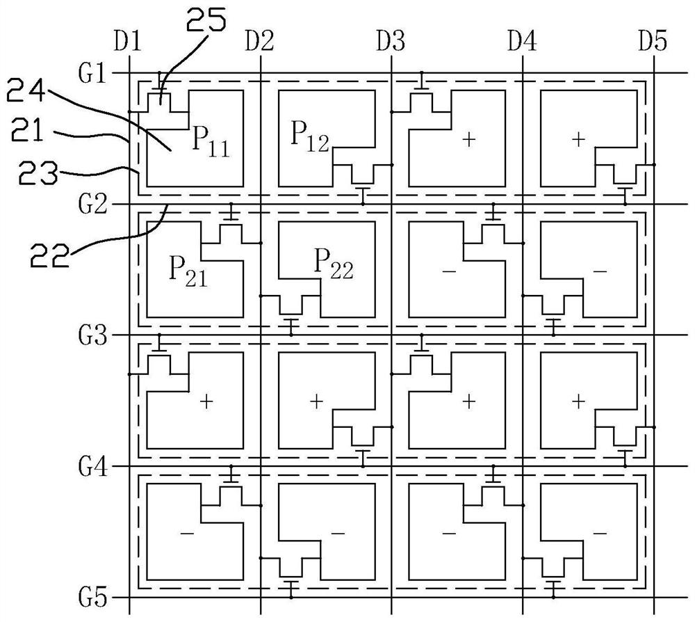
[0033] figure 2 A schematic structural diagram of an array substrate provided by an embodiment of the present invention. image 3 for figure 2 A schematic plan view of a group of pixel units in the array substrate shown. Figure 4 for image 3 A schematic plan view of two coupling electrodes in the group of pixel units shown. Figure 5 for image 3 A schematic plan view of two pixel electrodes in the group of pixel units is shown. Figure 6 for along image 3 Schematic cross-sectional view of line IV-IV. Please refer to Figure 2 to Figure 6 The array substrate 100 includes a plurality of scan lines 111 , a plurality of data lines 112 , a plurality of pixel electrodes 113 , a plurality of common electrode strips 115 and a plurality of coupling electrodes 116 disposed on the base substrate 110 .

[0034] A plurality of scanning lines 111 and a plurality of data lines 112 are insulated from each other and intersect to define a plurality of pixel units P arranged in an ...

no. 2 example

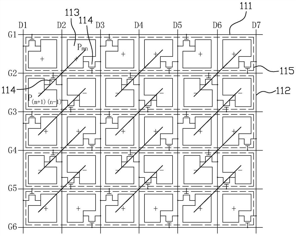
[0050] Please refer to Figure 8 and Figure 9 The difference between the array substrate provided by the second embodiment of the present invention and the above-mentioned first embodiment is that in this embodiment, the pixel units P in odd columns in each row are connected to the scanning lines 111 on the lower side of the pixel units P in the row, The pixel unit P in the even column is connected to the scanning line 111 on the upper side of the pixel unit P in the row, the pixel unit P in the odd row and the odd column is connected to the data line 112 on the left side of the pixel unit P in the column, and is located in the even column of the odd row The pixel unit P in the column is connected to the data line 112 on the right side of the pixel unit P in the column, the pixel unit P in the even row and the odd column is connected to the data line 112 on the right side of the pixel unit P in the column, and the pixel unit P in the even row and even column It is connected ...


PUM


Abstract

An array substrate and a liquid crystal display device, the array substrate is provided with scanning lines, data lines, a plurality of pixel electrodes, a plurality of common electrode strips and a plurality of coupling electrodes, the plurality of coupling electrodes, the common electrode strips and the plurality of coupling electrodes The three pixel electrodes are spaced apart from each other, the plurality of coupling electrodes are located below the plurality of pixel electrodes, the plurality of common electrode strips are located between the plurality of coupling electrodes and the plurality of pixel electrodes, and in each pixel unit A pixel electrode and a coupling electrode are provided. In each group of pixel units P, the pixel electrodes in the first pixel unit Pmn are conductively connected to the drain electrodes in the pixel unit through the first contact hole, and the coupling electrodes in the first pixel unit Pmn The electrode is electrically connected to the pixel electrode in the second pixel unit P(m+1)(n-1) through the second contact hole, and the coupling electrode in the second pixel unit P(m+1)(n-1) is connected through the second pixel unit P(m+1)(n-1). A contact hole is conductively connected to the pixel electrode in the first pixel unit Pmn, and the pixel electrode in the second pixel unit P(m+1)(n-1) is conductively connected to the drain in this pixel unit.

Description

technical field [0001] The invention relates to the technical field of liquid crystal display, in particular to an array substrate and a liquid crystal display device. Background technique [0002] Most of the liquid crystal display devices currently on the market are backlight liquid crystal display devices, which include a liquid crystal display panel and a backlight module. Usually, the liquid crystal display panel consists of a color filter substrate (CF, Color Filter), a thin film transistor array substrate (TFT, Thin Film Transistor), a liquid crystal (LC, Liquid Crystal) sandwiched between the color filter substrate and the thin film transistor array substrate, and a sealing frame. Glue (Sealant) composition. [0003] At present, the TFT-LCD display panels on the mainstream market can be divided into three types, namely twisted nematic (Twisted nematic, Tn) or super twisted nematic (Super Twisted nematic, STn) type, in-plane switching (In- Plane Switching (IPS) type...

Claims


Application Information

Patent Timeline
Patent Type & Authority Patents(China)
IPC IPC(8): G02F1/1343G02F1/1362
CPCG02F1/134309G02F1/136286
Inventor 乔艳冰付佃力
Owner KUSN INFOVISION OPTOELECTRONICS
Why Eureka
Try Eureka