A shielding grid mosfet
A shielding gate and control gate technology, applied in semiconductor devices, electrical components, circuits, etc., can solve problems such as device damage, reliability problems, and device failure, so as to improve reliability, eliminate the possibility of conduction, and avoid secondary The effect of a breakdown
- Summary
- Abstract
- Description
- Claims
- Application Information
AI Technical Summary
Problems solved by technology
Method used
Image

Examples
Embodiment 1
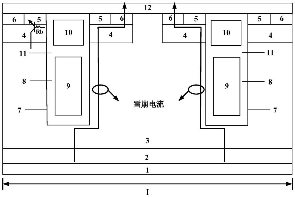
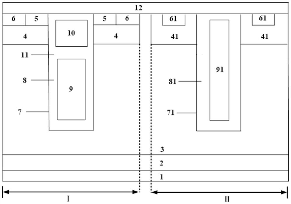
[0026] This embodiment provides a shielded gate MOSFET, such as figure 2 As shown, it includes a metallized drain 1 and a semiconductor substrate 2 of the first conductivity type that are sequentially stacked from bottom to top. The first conductivity type semiconductor drift region 3 and the metallized source 12; characterized in that, the first conductivity type semiconductor drift region 3 is provided with a working cell region and a leakage cell region;
[0027]The working cell region includes: a second conductivity type semiconductor body region-4, a first conductivity type semiconductor heavily doped source region-5, a second conductivity type semiconductor heavily doped contact region-6, a first shielding gate structure and The first control gate structure; the second conductivity type semiconductor body region-4 is arranged on both sides of the top layer of the first conductivity type semiconductor drift region 3; the first conductivity type semiconductor heavily dope...
Embodiment 2
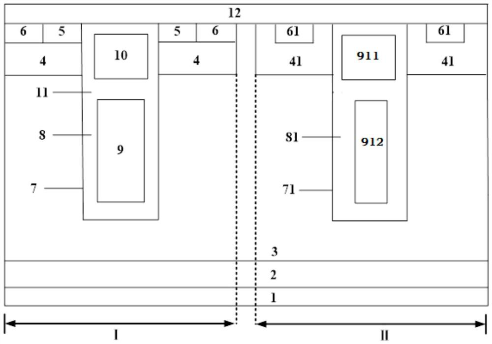
[0035] This embodiment provides a shielded gate MOSFET, such as image 3 As shown, the difference between this embodiment and Embodiment 1 is that the second shielding grid electrode 91 in the discharge cell can be designed as two mutually independent first split shielding grid electrodes 911 and second split shielding grid electrodes 912, The first split shielding gate electrode 911 is disposed above the second split shielding gate electrode 912 , and the depth of the first split shielding gate electrode 911 is greater than the junction depth of the second conductivity type semiconductor body region 2 41 . The first split shielding gate electrode 911 is structurally equivalent to the first control gate electrode 10 in the working cell region, but since there is no source region in the leakage cell region, the first split shielding gate electrode 911 does not have the function of turning on A dielectric layer may be used to isolate the first split shielding gate electrode 911 ...
Embodiment 3
[0038] This embodiment provides a shielded gate MOSFET, such as Figure 7 As shown, the difference between this embodiment and Embodiment 1 is that the second shielding grid electrode 91 of the discharge cell can be designed as two mutually independent first split shielding grid electrodes 911 and second split shielding grid electrodes 912, The first split shielding gate electrode 911 is disposed above the second split shielding gate electrode 912 , and the depth of the first split shielding gate electrode 911 is greater than the junction depth of the second conductivity type semiconductor body region 2 41 . The first split shielding gate electrode 911 is structurally equivalent to the first control gate electrode 10 in the working cell region, but since there is no source region in the leakage cell region, the first split shielding gate electrode 911 does not have the function of turning on , and precisely because of this, the first split shielding gate electrode 911 and the ...
PUM
 Abstract
Description
Claims
Application Information
 - R&D
- Intellectual Property
- Life Sciences
- Materials
- Tech Scout
- Unparalleled Data Quality
- Higher Quality Content
- 60% Fewer Hallucinations
Browse by: Latest US Patents, China's latest patents, Technical Efficacy Thesaurus, Application Domain, Technology Topic, Popular Technical Reports.
© 2025 PatSnap. All rights reserved.Legal|Privacy policy|Modern Slavery Act Transparency Statement|Sitemap|About US| Contact US: help@patsnap.com