Semiconductor device and preparation method thereof

A semiconductor and device technology, which is applied in the field of semiconductor devices and their preparation, can solve the problem of single switching characteristics and achieve the effect of easy adjustment

Inactive Publication Date: 2019-01-04
GLOBAL ENERGY INTERCONNECTION RES INST CO LTD +2
View PDF4 Cites 2 Cited by
  • Summary
  • Abstract
  • Description
  • Claims
  • Application Information

AI Technical Summary

Problems solved by technology

[0006] In view of this, an embodiment of the present invention provides a semiconductor device and a manufacturing method thereof to solve the problem of single switching characteristics of existing semiconductor devices

Method used


Image

  • Semiconductor device and preparation method thereof
  • Semiconductor device and preparation method thereof
  • Semiconductor device and preparation method thereof

Examples


Embodiment Construction

[0051] The technical solutions of the present invention will be clearly and completely described below in conjunction with the accompanying drawings. Apparently, the described embodiments are some of the embodiments of the present invention, but not all of them. Based on the embodiments of the present invention, all other embodiments obtained by persons of ordinary skill in the art without making creative efforts belong to the protection scope of the present invention.

[0052] In the description of the present invention, it should be noted that the terms "first", "second", and "third" are used for description purposes only, and should not be understood as indicating or implying relative importance.

[0053] In addition, the technical features involved in the different embodiments of the present invention described below may be combined with each other as long as there is no conflict with each other.

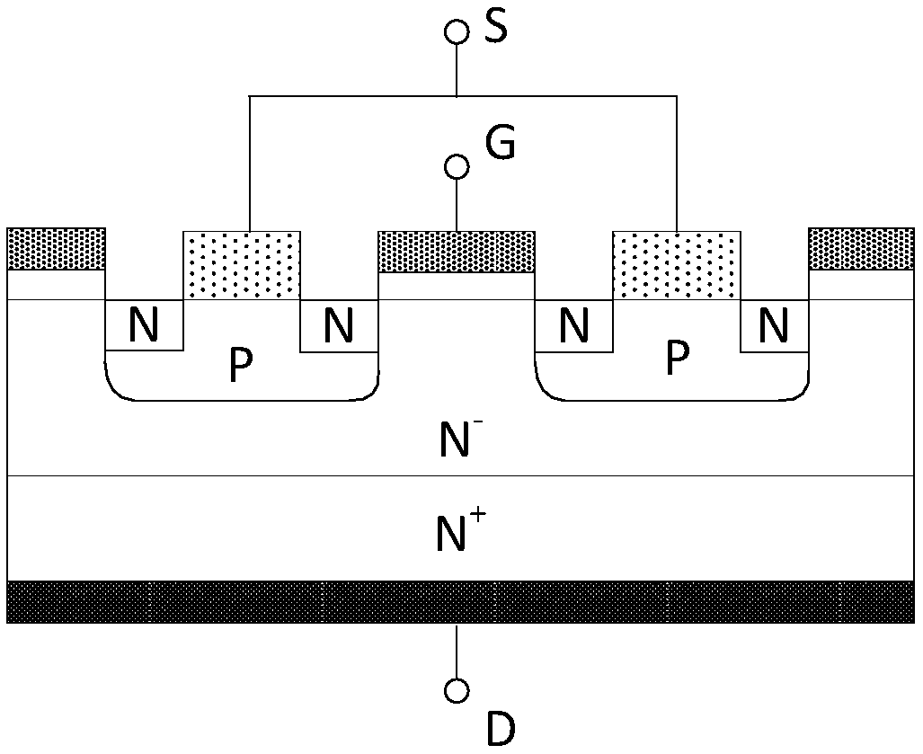
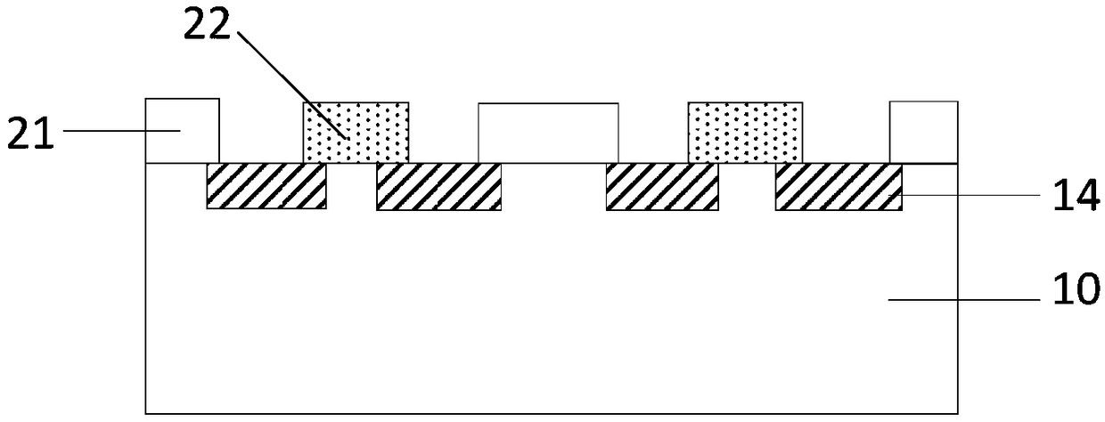
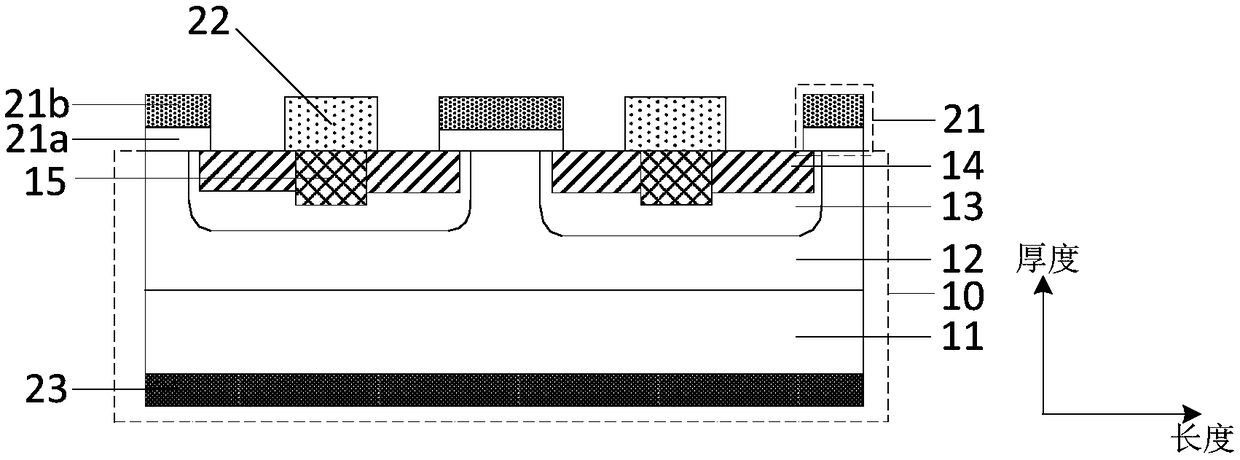
[0054] An embodiment of the present invention provides a semiconductor devi...


PUM


Abstract

The invention relates to the technical field of semiconductors, and provides a semiconductor device and a preparation method thereof, wherein, the semiconductor device comprises a semiconductor layer;a gate electrode and a source electrode formed over the semiconductor layer; A semiconductor region formed in the semiconductor layer between the gate electrode and the source electrode, and having aportion overlapping with the gate electrode and/or the source electrode; Wherein the ion doping concentration in the semiconductor region is 1E16-5E21cm<-3>, that conductivity type of the semiconductor region is the same as that of the semiconductor lay. By forming a semiconductor region in the semiconductor layer between the gate electrode and the source electrode, The semiconductor region has aportion overlapping with the gate and/or the source, wherein the area of the overlapping portion may be used to change the MOS capacitance at the coincidence of the gate and/or the source, thereby realizing modulation of switching characteristics such as switching time and switching loss of the grid control semiconductor device.

Description

technical field [0001] The invention relates to the technical field of semiconductors, in particular to a semiconductor device and a preparation method thereof. Background technique [0002] Semiconductor devices are electronic devices that use the special electrical properties of semiconductor materials to complete specific functions, and can be used to generate, control, receive, transform, amplify signals and perform energy conversion. Among them, Metal-Oxide Semiconductor FET (MOSFET for short) is the most commonly used. [0003] Among them, in order to improve the electrical characteristics of MOS tubes, especially the ability to withstand voltage and current, most MOSFETs adopt vertical conductive structures, also known as VMOSFETs (Vertical MOSFETs). The specific structures are as follows: figure 1 As shown, it is commonly used as a switching element. [0004] However, different application fields such as rail transit, power grids, and photovoltaic inverters have di...

Claims


Application Information

Patent Timeline
Patent Type & Authority Applications(China)
IPC IPC(8): H01L29/78H01L21/336H01L21/265H01L21/266
CPCH01L29/66712H01L29/7802H01L21/26513H01L21/266H01L29/66068H01L21/047H01L29/086
Inventor 郑柳桑玲李嘉琳董少华金锐杨霏
Owner GLOBAL ENERGY INTERCONNECTION RES INST CO LTD
Why Eureka
Try Eureka