
Method of reducing tin soldering voidage between COB (chip on board) and heat-dissipation base

A technology of heat dissipation base and void rate, which is applied to tin feeding devices, welding equipment, auxiliary devices, etc., can solve the problems of inability to further improve the heat dissipation efficiency of the whole lamp and the high void rate of soldering, so as to ensure the industrialization promotion and improve the success. rate effect

Inactive Publication Date: 2018-12-25
厦门吉来特光电有限公司
View PDF0 Cites 5 Cited by
  • Summary
  • Abstract
  • Description
  • Claims
  • Application Information

AI Technical Summary

Problems solved by technology

[0006] The main purpose of the present invention is to provide a method for reducing the solder void rate between the COB board and the heat dissipation base, so as to solve the problem that the solder void rate of the prior art is too high when the COB board is welded on the heat dissipation base and cannot be further improved. The problem of improving the heat dissipation efficiency of the whole lamp

Method used


Image

  • Method of reducing tin soldering voidage between COB (chip on board) and heat-dissipation base
  • Method of reducing tin soldering voidage between COB (chip on board) and heat-dissipation base
  • Method of reducing tin soldering voidage between COB (chip on board) and heat-dissipation base

Examples


Embodiment Construction

[0030] In order to further explain the technical solution of the present invention, the present invention will be described in detail below through specific examples.

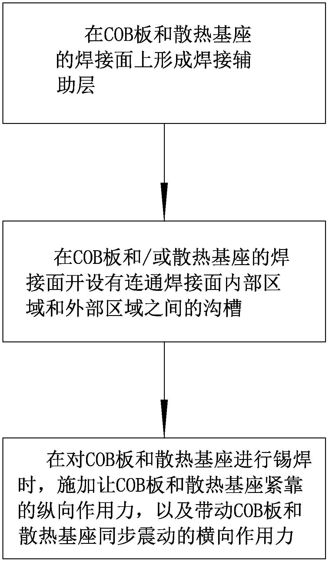
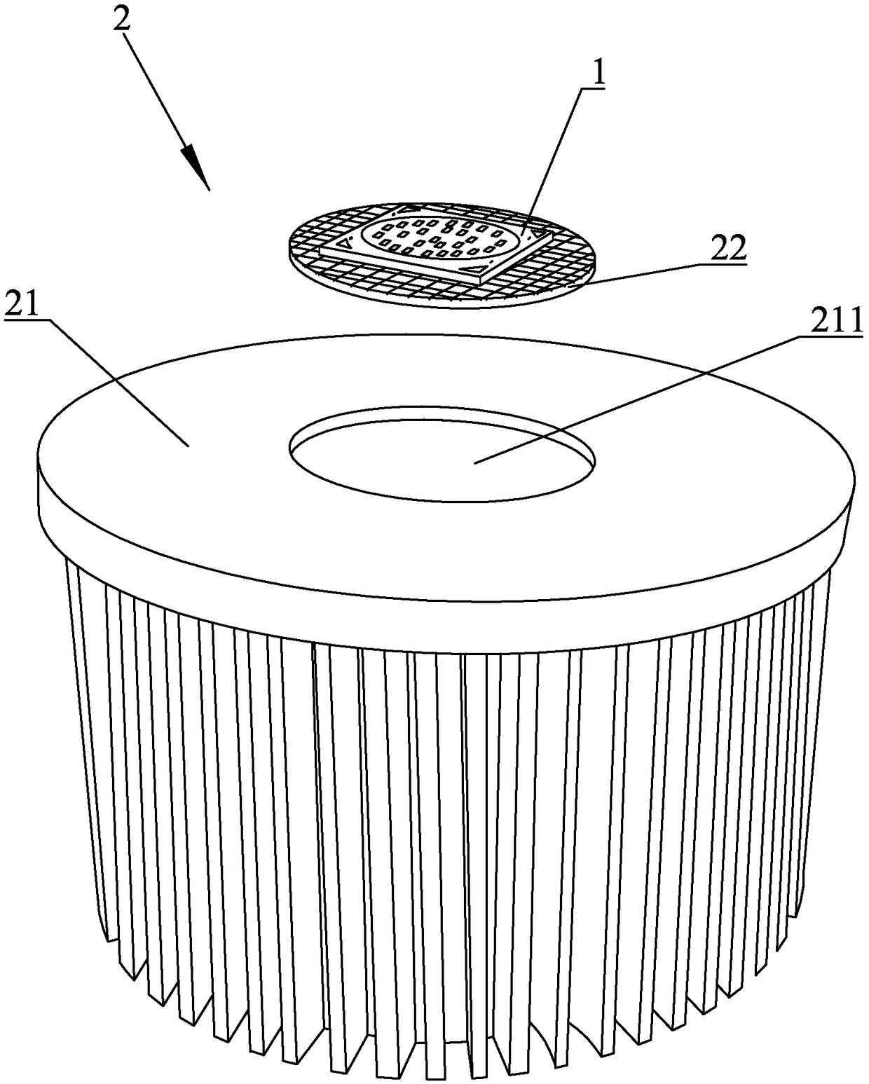
[0031] Such as Figure 2 to Figure 8 As shown, the present invention relates to a method for reducing the solder void rate between the COB board 1 and the heat dissipation base 2, comprising the following steps:

[0032] ① Form a welding auxiliary layer on the welding surface of the heat dissipation base 2; the welding auxiliary layer is to ensure that the melted solder paste will not cause desoldering due to the excessive thermal conductivity of the COB board 1 or the heat dissipation base 2; In this embodiment, the welding auxiliary layer is selected as a nickel-plated layer;

[0033] ② On the welding surface of the COB board 1 and / or the heat dissipation base 2, there is a groove connecting the inner area and the outer area of ​​the welding surface, the depth of the groove is greater than or equal to the th...


PUM


Abstract

The invention discloses a method of reducing tin soldering voidage between a COB (chip on board) and a heat-dissipation base. The method comprises the following steps of: (1) forming a soldering assistance layer on a soldering face of the heat-dissipation base, (2) forming a groove communicating an internal area and an external area of the soldering face in the COB or the soldering face of the heat-dissipation base, (3) applying a longitudinal acting force to allow the COB to close to the heat-dissipation base and a transverse acting force to drive the COB to rock during tin soldering of the COB and the heat-dissipation base, wherein the depth of the groove is greater than or equal to the thickness of the soldering assistance layer and less than the thickness sum of the soldering assistance layer and the COB or the heat-dissipation base. The method can greatly increase an actual soldering success rate; high efficiency of a heat conduction bridge between the COB and the heat-dissipationbase is guaranteed; and actual industrial popularization of the high-power COB is guaranteed.

Description

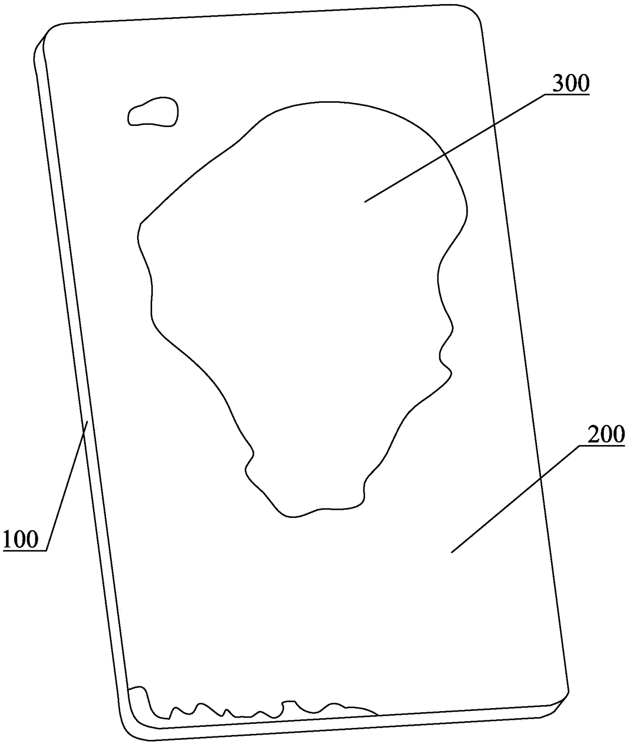
technical field [0001] The invention relates to the field of lamp manufacturing, in particular to a method for reducing the solder void rate between a COB board and a heat dissipation base. Background technique [0002] In the process of processing and forming lamps, welding operations are required. When soldering is often used in actual welding, refer to figure 1 , in the process of using solder paste, there may be solder voids 300 phenomenon. [0003] The formation of the above-mentioned welding void 300 is generally caused by flux or air. For example, the proportion of flux is too large, which makes it difficult for the flux to escape completely before the solder joint solidifies; The solvent is difficult to completely volatilize, and it will cause filling voids if it stays inside the solder joint; another example is the organic matter contaminated during the operation, or because the welding time is too short, the time for gas to escape is not enough, etc. [0004] For...

Claims


Application Information

Patent Timeline
IPC IPC(8): B23K3/06B23K3/08
CPCB23K3/08B23K3/0607
Inventor 张智丰黄泓豪陈必为
Owner 厦门吉来特光电有限公司
Learn More