Flexible display device and manufacturing method thereof
A flexible display and device technology, used in semiconductor/solid-state device manufacturing, semiconductor devices, electric solid-state devices, etc., can solve the problem of inability to block the side penetration of water vapor
- Summary
- Abstract
- Description
- Claims
- Application Information
AI Technical Summary
Problems solved by technology
Method used
Image
Examples
preparation example Construction
[0058] The above-mentioned preparation method of a flexible display device comprises the following steps:
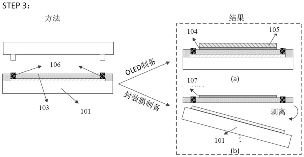
[0059] A first carrier substrate is provided, a polyimide solution is coated on the surface of the first carrier substrate, and cured to form the flexible film substrate; the surface of the flexible film substrate includes a device area and a first packaging area, and the surface of the first carrier substrate An encapsulation area forms a first annular groove, and the first annular groove is filled with nano glass paste;
[0060] forming an electroluminescent component in the device region;
[0061] A second carrier substrate is provided, a polyimide solution is coated on the surface of the second carrier substrate, and cured to form the flexible packaging substrate; the surface of the flexible packaging substrate is provided with a first groove corresponding to the first annular groove. Two annular grooves, the second annular groove is filled with nano glass paste; pe...
Embodiment
[0069] A flexible display device in this embodiment includes:
[0070] A flexible film substrate (it can be understood that the material is preferably polyimide), the surface of the flexible film substrate includes a device area and a first packaging area, and the first packaging area is provided with a first annular groove;
[0071] A flexible packaging substrate, the surface of the flexible packaging substrate is provided with a second annular groove corresponding to the first annular groove;
[0072] An electroluminescent component (understandably, it may be an OLED), stacked on the device region;
[0073] Both the first annular groove and the second annular groove are filled with nano glass paste, and the nano glass paste in the first annular groove and the second annular groove is melted to form a nano glass paste melting part, The flexible film substrate and the flexible packaging substrate are integrated, and the electroluminescence component is packaged between the fl...
PUM
| Property | Measurement | Unit |
|---|---|---|
| depth | aaaaa | aaaaa |
| width | aaaaa | aaaaa |
Abstract
Description
Claims
Application Information
 - R&D Engineer
- R&D Manager
- IP Professional
- Industry Leading Data Capabilities
- Powerful AI technology
- Patent DNA Extraction
Browse by: Latest US Patents, China's latest patents, Technical Efficacy Thesaurus, Application Domain, Technology Topic, Popular Technical Reports.
© 2024 PatSnap. All rights reserved.Legal|Privacy policy|Modern Slavery Act Transparency Statement|Sitemap|About US| Contact US: help@patsnap.com


