A kind of crosslinked nanoparticle film and preparation method and thin film optoelectronic device

A technology of optoelectronic devices and nanoparticles, which is applied in the direction of electrical components, photovoltaic power generation, semiconductor devices, etc., can solve the problems of low carrier mobility and high carrier transport barriers, and achieve increased electrical coupling, lower potential barriers, Performance-enhancing effects

Active Publication Date: 2020-05-05
TCL CORPORATION
View PDF5 Cites 0 Cited by
  • Summary
  • Abstract
  • Description
  • Claims
  • Application Information

AI Technical Summary

Problems solved by technology

[0005] In view of the above-mentioned deficiencies in the prior art, the object of the present invention is to provide a cross-linked nanoparticle film and its preparation method and thin-film optoelectronic device, aiming to solve the problem that the carrier transport barrier of the existing device film is relatively high, and the carrier migration low rate problem

Method used


Image

  • A kind of crosslinked nanoparticle film and preparation method and thin film optoelectronic device
  • A kind of crosslinked nanoparticle film and preparation method and thin film optoelectronic device
  • A kind of crosslinked nanoparticle film and preparation method and thin film optoelectronic device

Examples


Embodiment Construction

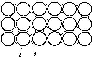
[0031] The present invention provides a cross-linked nanoparticle thin film, a preparation method and a thin film optoelectronic device. In order to make the purpose, technical solution and effect of the present invention clearer and clearer, the present invention will be further described in detail below. It should be understood that the specific embodiments described here are only used to explain the present invention, not to limit the present invention.

[0032] A preferred embodiment of the preparation method of a cross-linked nanoparticle film of the present invention, including:

[0033] Step A, dispersing the nanoparticles in a solvent, and stirring evenly to obtain a nanoparticle solution;

[0034] The step A is specifically to disperse the nanoparticles in the solvent at a mass concentration of 1-100 mg / ml, and stir until they are evenly mixed to prepare a nanoparticle solution that can be used for film formation by the solution method. Wherein, the nanoparticles can...


PUM

PropertyMeasurementUnit
diameteraaaaaaaaaa
thicknessaaaaaaaaaa

Abstract

The invention discloses a cross-linked nanoparticle film and amanufacturing method thereof, and a thin film optoelectronic device. The method comprises the following steps of dispersing nanoparticlesin a solvent, stirring uniformly and acquiring a nanoparticle solution; and through a solution method, manufacturing the nanoparticle solution into a nanoparticle film, injecting a combined gas to urge cross-linked reaction generation, and acquiring the cross-linked nanoparticle film. In the invention, when the nanoparticles form a film, the combined gas is injected so that the particles are urgedto carry out mutual crosslinking. Therefore, the electrical coupling among the particles is increased, the barrier of carrier transmission is reduced, a carrier mobility is increased, and electric performance is greatly improved.

Description

technical field [0001] The invention relates to the field of device thin film preparation, in particular to a cross-linked nanoparticle thin film, a preparation method and a thin film optoelectronic device. Background technique [0002] Oxide nanoparticles (or spherical oxide nanocrystals) have a good degree of crystallinity, which ensures their optical and electrical properties similar to those of bulk materials (low-dimensional materials); on the other hand, due to the self-assembly of nanoparticles into films Very well, so that a low-cost coating preparation process can be applied. In the process of optoelectronic devices prepared by solution method, nanoparticles are one of the important solutions to form the corresponding oxide thin films. Common examples include zinc oxide (ZnO x ) nanoparticles, titanium oxide (TiO x ) Thin films of particles are used as semiconductor materials for transporting electrons in light-emitting diodes, thin-film solar cells, and thin-fil...

Claims


Application Information

Patent Timeline
Patent Type & Authority Patents(China)
IPC IPC(8): H01L21/02H01L33/00H01L29/786H01L31/08
CPCH01L21/0254H01L21/02554H01L21/02557H01L21/0256H01L21/02601H01L21/02628H01L29/786H01L31/0445H01L31/08H01L33/00Y02E10/50
Inventor 陈崧钱磊杨一行曹蔚然向超宇
Owner TCL CORPORATION
Why Eureka
Try Eureka