
Method and device for correcting exposure pattern, and exposure equipment

A technique for exposing patterns and original designs, which can be applied in microlithography exposure equipment, photolithography exposure equipment, photomechanical equipment, etc., and can solve the problem of high cost

Inactive Publication Date: 2020-06-05
BOE TECH GRP CO LTD +1
View PDF8 Cites 0 Cited by
  • Summary
  • Abstract
  • Description
  • Claims
  • Application Information

AI Technical Summary

Problems solved by technology

[0006] Embodiments of the present invention provide a method and device for correcting exposure patterns, and exposure equipment, which are used to avoid the high cost of reducing the difference between the TP design value and the actual value of the exposure pattern of the color filter substrate by replacing the mask plate. high problem

Method used


Image

  • Method and device for correcting exposure pattern, and exposure equipment
  • Method and device for correcting exposure pattern, and exposure equipment
  • Method and device for correcting exposure pattern, and exposure equipment

Examples


Embodiment Construction

[0027] The technical solutions in the embodiments of the present invention will be clearly and completely described below in conjunction with the accompanying drawings in the embodiments of the present invention. Obviously, the described embodiments are only a part of the embodiments of the present invention, rather than all the embodiments. Based on the embodiments of the present invention, all other embodiments obtained by those of ordinary skill in the art without creative work shall fall within the protection scope of the present invention.

[0028] The embodiment of the present invention provides a method for correcting an exposure pattern. Optionally, the method for correcting includes: obtaining at least one first measurement size and a corresponding second measurement size of the exposure pattern on the base substrate. as well as:

[0029] Step 101: Compensate the original design coordinates of the workbench relative to the mask according to at least one first measurement s...


PUM


Abstract

The invention provides an exposure pattern compensation method, an exposure pattern compensationdevice and exposure equipment, and relates to the field of display panel manufacturing. The method, thedevice and the equipment are used for solving the problem of high cost during the TP deign value and practical value difference reduction of the color film base plate exposure pattern in a mask platereplacing mode in the prior art. The compensation method comprises the following steps of compensating the original design coordinate of a work table relative to a mask plate according to at least onefirst measurement dimension, corresponding second measurement dimension, the corresponding design dimension and the threshold value work coefficient, so that the compensation design coordinate of thework table relative to the mask plate can be obtained; controlling the movement of the work table relative to the mask plate according to the compensation design coordinate. The first measuring dimension is the exposure pattern dimension measured after the formation of the exposure pattern; the second measurement dimension is the dimension of the exposure pattern measured after the formation of other patterns on the substrate base plate; the design dimension is the design dimension of the exposure pattern.

Description

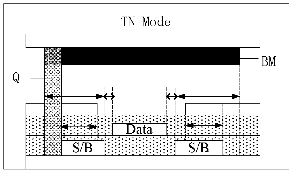
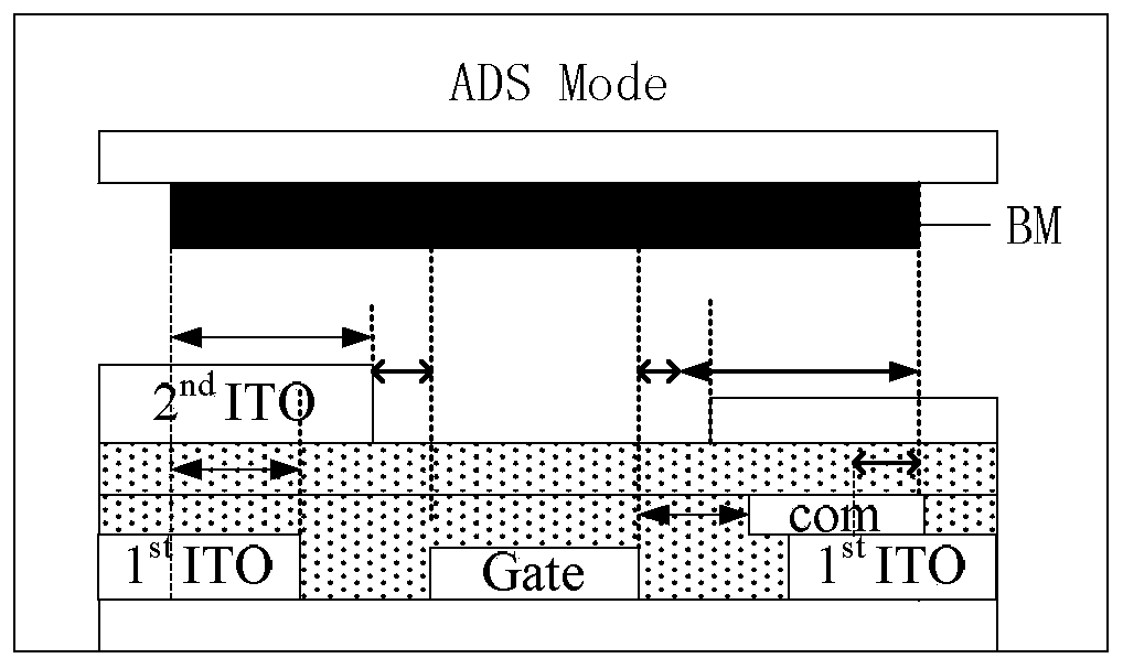
Technical field [0001] The present invention relates to the field of display panel manufacturing, in particular to a method and device for correcting exposure patterns, and exposure equipment. Background technique [0002] In the TFT-LCD manufacturing process, whether it is TN type (Twisted Nematic Mode, twisted nematic) or ADS type (Advanced-Super Dimension Switch Mode, advanced super dimensional field switch) products, there are Touch Mura (apply a certain amount on the surface of the finished module). External force, the phenomenon of white and bright under the dark state picture) problem. Since the formation principle of Touch Mura is more complicated and there are many influencing factors, this defect has always been a problem in the industry. According to the research of Touch Mura mechanism, its influencing factors are generally summarized as the following two: [0003] figure 1 It is a structural diagram of a TN Mode liquid crystal panel, which is mainly due to the uneven...

Claims


Application Information

Patent Timeline
Patent Type & Authority Patents(China)
IPC IPC(8): G03F7/20
CPCG03F7/70308G03F7/70733
Inventor 周鹏蒋迁孟令剑章旭
Owner BOE TECH GRP CO LTD
Learn More