Pixel structure and display device

A pixel structure and pixel technology, applied in semiconductor devices, electrical components, circuits, etc., can solve problems such as uneven service life and unfavorable material life, and achieve the effect of improving service life, improving display effect, and uniform pixel arrangement.

Active Publication Date: 2019-07-26
KUNSHAN GO VISIONOX OPTO ELECTRONICS CO LTD
View PDF4 Cites 0 Cited by
  • Summary
  • Abstract
  • Description
  • Claims
  • Application Information

AI Technical Summary

Problems solved by technology

[0004] However, at present, the blue sub-pixel in the OLED display device is a fluorescent material, and the red sub-pixel and green sub-pixel are phosphorescent materials. Due to the limitation of the material, the luminous life of the red sub-pixel is higher than that of the green sub-pixel, and the red sub-pixel is higher than the green sub-pixel. The pixels are much higher than the blue sub-pixels, and the service life of the materials of the three sub-pixels is not balanced
[0005] The existing pixel arrangement is also not conducive to the balance of the current material life, and, with the development of display panels to high resolution, how to arrange the pixels to improve the resolution and balance the material life is a problem that those skilled in the art need to solve technical issues

Method used


Image

  • Pixel structure and display device
  • Pixel structure and display device
  • Pixel structure and display device

Examples


Embodiment 1

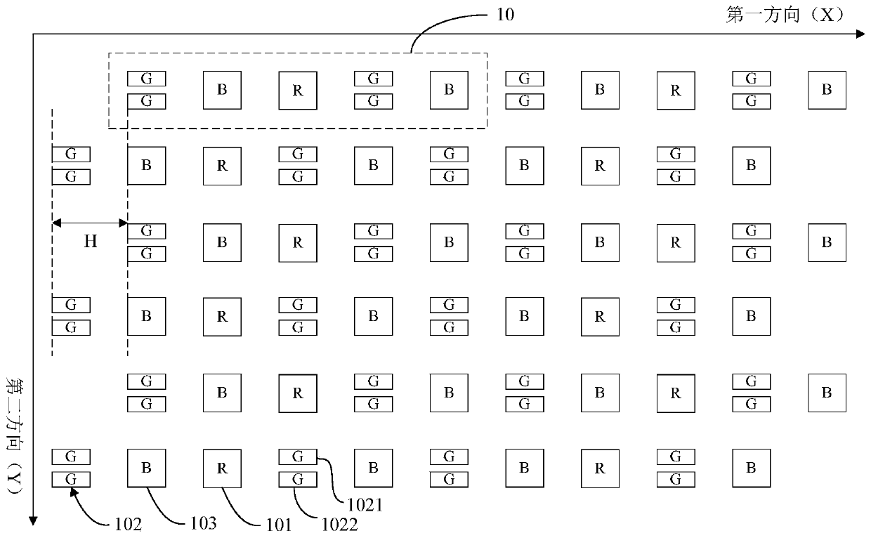
[0043] figure 1It is a schematic structural diagram of the pixel structure provided by Embodiment 1 of the present invention. For simplicity, only a part of the pixel structure is shown in the drawings, and the number of pixels in an actual product is not limited thereto, and the number of pixel units can be changed accordingly according to actual display requirements.

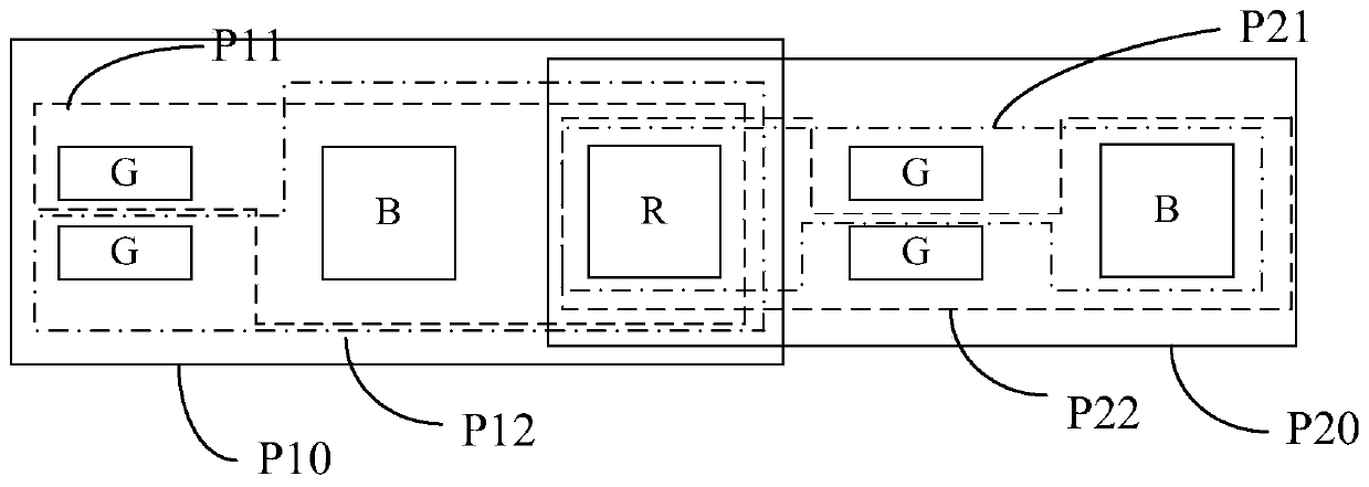
[0044] Such as figure 1 As shown, the present invention provides a pixel structure, including a plurality of repeating units 10 arranged in a matrix, the repeating units 10 are repeatedly arranged along the first direction and the second direction, and each repeating unit 10 includes One first sub-pixel 101, two second sub-pixels 102 and two third sub-pixels 103 are arranged, the first sub-pixel 101 is located in the middle, and the second sub-pixel 102 and the third sub-pixel 103 are respectively located Two sides of the first sub-pixel 101 , and among the three sub-pixels, one sub-pixel whose brightness is...

Embodiment 2

[0059] image 3 It is a schematic structural diagram of the pixel structure provided by Embodiment 2 of the present invention. Such as image 3 As shown, the present invention provides a pixel structure, including a plurality of repeating units 10 arranged in a matrix, the repeating units 10 are repeatedly arranged along the first direction and the second direction, and each repeating unit 10 includes One first sub-pixel 101, two second sub-pixels 102 and two third sub-pixels 103 are arranged, the first sub-pixel 101 is located in the middle, and the second sub-pixel 102 and the third sub-pixel 103 are respectively located Two sides of the first sub-pixel 101 , and among the three sub-pixels, one sub-pixel whose brightness is higher than the remaining two sub-pixels is divided into two subordinate sub-pixels in the second direction.

[0060] The difference between this embodiment and Embodiment 1 is that in this embodiment, the repeating unit 10 includes a third sub-pixel 10...

Embodiment 3

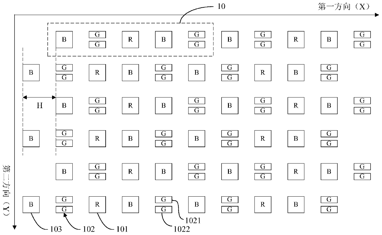
[0066] Figure 5 It is a schematic structural diagram of the pixel structure provided by the third embodiment of the present invention. For simplicity, only a part of the pixel structure is shown in the drawings, and the number of pixels in an actual product is not limited thereto, and the number of pixel units can be changed accordingly according to actual display requirements.

[0067] Such as Figure 5 As shown, the present invention provides a pixel structure, including a plurality of repeating units 10 arranged in a matrix, the repeating units 10 are repeatedly arranged along the first direction and the second direction, and each repeating unit 10 includes Three sub-pixels with different colors are arranged, wherein the repeating unit 10 includes a first sub-pixel 101, two second sub-pixels 102 and two third sub-pixels 103, and the first sub-pixel 101 is located in the middle , the second sub-pixel 102 and the third sub-pixel 103 are respectively located on both sides o...


PUM


Abstract

The present invention provides a pixel structure and a display device. The pixel structure includes a plurality of repeating units arranged in an array, and each repeating unit includes a plurality of sub-pixels with three colors, wherein one color has one sub-pixel, and the other two There are two sub-pixels of each color, which are respectively located on both sides of the sub-pixel of one color, and the sub-pixel in the middle forms two pixel units with the two sub-pixels on both sides, so that the sharing of sub-pixels is realized. It is conducive to improving the resolution of the display device; among the sub-pixels of the three colors, the sub-pixel with the highest brightness is divided into two subordinate sub-pixels, so that the number of sub-pixels with the highest brightness increases, thereby increasing the PPI and improving the resolution of the display device , at the same time, the same opening of the evaporation mask can be used to evaporate two separated sub-pixels at the same time, which can reduce the difficulty of the manufacturing process of the evaporation mask and the evaporation process.

Description

technical field [0001] The present invention relates to the technical field of plane display, in particular to a pixel structure and a display device. Background technique [0002] Organic Light-Emitting Diode (OLED) display device is one of the hotspots in the field of flat panel display research today. Compared with Liquid Crystal Display (LCD), OLED display device has wide viewing angle, high brightness, high Contrast, low power consumption, thinner and lighter volume and other advantages. At present, OLED display devices have begun to replace traditional liquid crystal displays in the fields of flat panel displays such as mobile phones, personal digital assistants (PDAs), and digital cameras. [0003] The structure of the OLED display device mainly includes: a base substrate, and pixels arranged in a matrix on the base substrate. Wherein, each pixel generally forms an organic electroluminescent structure at a corresponding pixel position on the array substrate through ...

Claims


Application Information

Patent Timeline
Patent Type & Authority Patents(China)
IPC IPC(8): H01L27/32
CPCH10K59/353
Inventor 刘明星李俊峰王徐亮高峰
Owner KUNSHAN GO VISIONOX OPTO ELECTRONICS CO LTD
Why Eureka
Try Eureka