


Quick Research
Generate reliable direction feasibility study reports for your R&D in just a few steps.

Technical Q&A
Discover and master advanced knowledge NOW. Basics, ideas, possibilities, all at once.

Find Solutions
As an expert in R&D theories, this can generate solutions to your technical problems instantly.

Evaluate Feasibility
Analyze your overall solution with one click, know your potential R&D risks in advance.

Monitor Landscape
Get weekly tech updates, stay abreast of the latest tech innovations and key insights.
A Printing Method of Functional Micro-Nano Heterostructure
A printing method and heterostructure technology, which is applied in the printing field of functional micro-nano heterostructures, can solve the problems of chaotic connection methods of heterogeneous structures, difficulty in controlling solutions, etc., and achieve the effect of precise and controllable interface morphology
- Summary
- Abstract
- Description
- Claims
- Application Information
AI Technical Summary
Problems solved by technology
Method used
Image

Examples
Embodiment 1
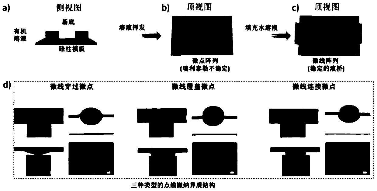
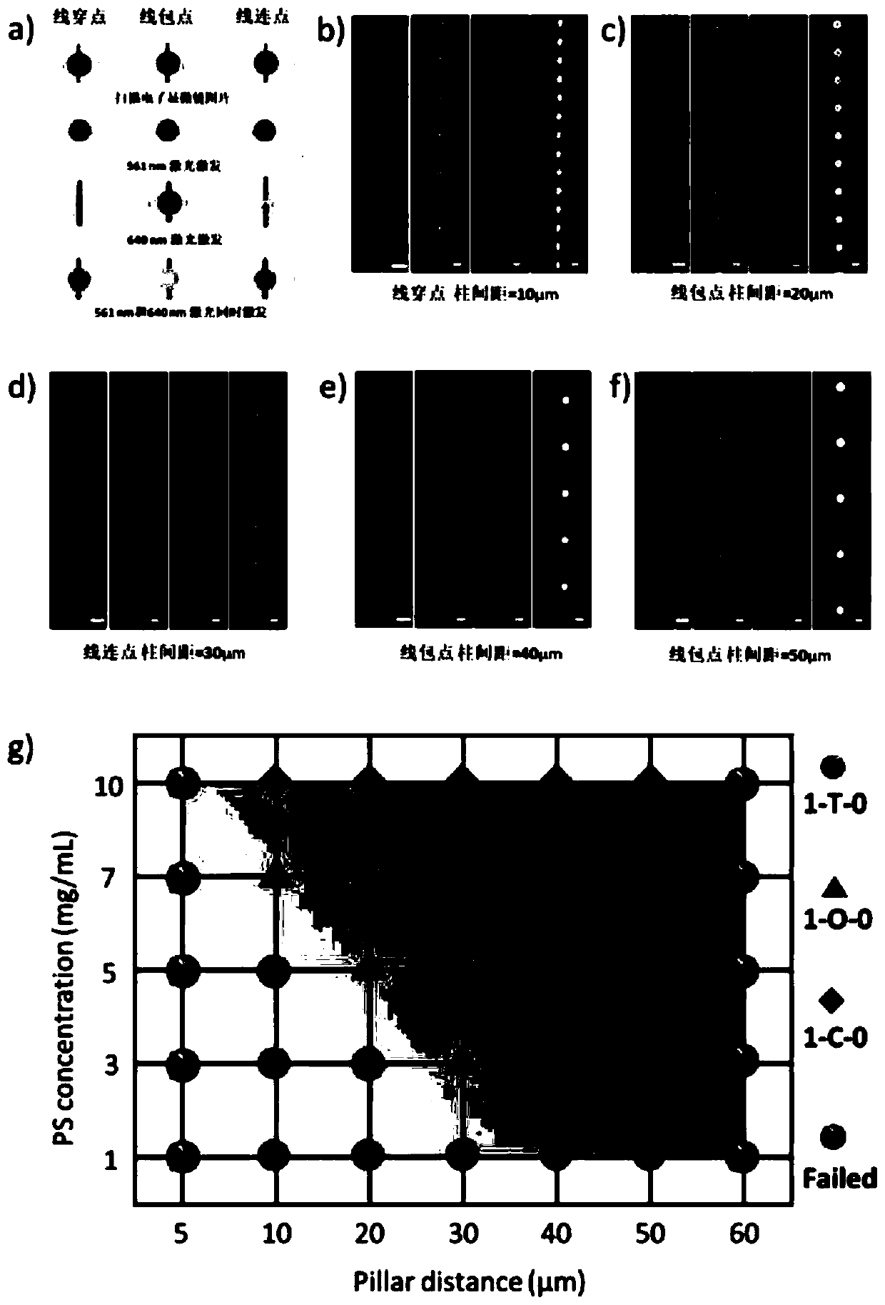
[0039] The mass content of CdS prepared by CdS quantum dots with a particle size of 5nm, polystyrene and o-dichlorobenzene is 0.2%, the mass content of polystyrene is 0.1%, and the balance is o-dichlorobenzene. Take 10 microliters from the liquid gun and spread it evenly on the photolithographic circular silicon column template; cover the silicon substrate on the silicon column template covered with the assembly solution, and let the solvent evaporate evenly at 80°C; take out the device and let it cool at room temperature, and again Inject 10 microliters of the assembly solution prepared by CdS quantum dots with a particle size of 5nm, polyvinyl alcohol, sodium lauryl sulfate and water, wherein the mass content of CdS is 0.2%, and the mass content of polyvinyl alcohol is 0.5%. The mass content of sodium alkyl sulfate is 0.2%, and the balance is water, so that the solvent is uniformly volatilized at 50° C., and after the water in the assembly solution volatilizes, a silicon wafe...
Embodiment 2
[0041] The mass content of CdS prepared by CdS quantum dots with a particle size of 5nm, polystyrene and o-dichlorobenzene is 0.2%, the mass content of polystyrene is 0.5%, and the balance is o-dichlorobenzene. Take 10 microliters from the liquid gun and spread it evenly on the photolithographic circular silicon column template; cover the silicon substrate on the silicon column template covered with the assembly solution, and let the solvent evaporate evenly at 80°C; take out the device and let it cool at room temperature, and again Inject 10 microliters of the assembly solution prepared by CdS quantum dots with a particle size of 5nm, polyvinyl alcohol, sodium lauryl sulfate and water, wherein the mass content of CdS is 0.2%, and the mass content of polyvinyl alcohol is 0.5%. The mass content of sodium alkyl sulfate is 0.2%, and the balance is water, so that the solvent is uniformly volatilized at 50° C., and after the water in the assembly solution volatilizes, the silicon ch...
Embodiment 3
[0043] The mass content of CdS prepared by CdS quantum dots with a particle size of 5nm, polystyrene and o-dichlorobenzene is 0.2%, the mass content of polystyrene is 1%, and the balance is o-dichlorobenzene. Take 10 microliters from the liquid gun and spread it evenly on the photolithographic circular silicon column template; cover the silicon substrate on the silicon column template covered with the assembly solution, and let the solvent evaporate evenly at 80°C; take out the device and let it cool at room temperature, and again Inject 10 microliters of the assembly solution prepared by CdS quantum dots with a particle size of 5nm, polyvinyl alcohol, sodium lauryl sulfate and water, wherein the mass content of CdS is 0.2%, and the mass content of polyvinyl alcohol is 0.5%. The mass content of sodium alkyl sulfate is 0.2%, and the balance is water, so that the solvent is uniformly volatilized at 50°C, and after the water in the assembly solution is volatilized, a micro-nano st...
PUM
| Property | Measurement | Unit |
|---|---|---|
| particle diameter | aaaaa | aaaaa |
| particle diameter | aaaaa | aaaaa |
| particle diameter | aaaaa | aaaaa |
Abstract
Description
Claims
Application Information
 - R&D Engineer
- R&D Manager
- IP Professional
- Industry Leading Data Capabilities
- Powerful AI technology
- Patent DNA Extraction
Browse by: Latest US Patents, China's latest patents, Technical Efficacy Thesaurus, Application Domain, Technology Topic, Popular Technical Reports.
© 2024 PatSnap. All rights reserved.Legal|Privacy policy|Modern Slavery Act Transparency Statement|Sitemap|About US| Contact US: help@patsnap.com