Electroluminescent display panel, manufacturing method and display device
An electroluminescent display and manufacturing method technology, applied in circuits, electrical components, static indicators, etc., can solve the problems of difficult process, high difficulty and high cost, and achieve the effect of eliminating the problem of aliasing display.
- Summary
- Abstract
- Description
- Claims
- Application Information
AI Technical Summary
Problems solved by technology
Method used
Image
Examples
Embodiment Construction
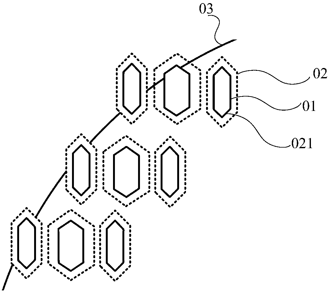
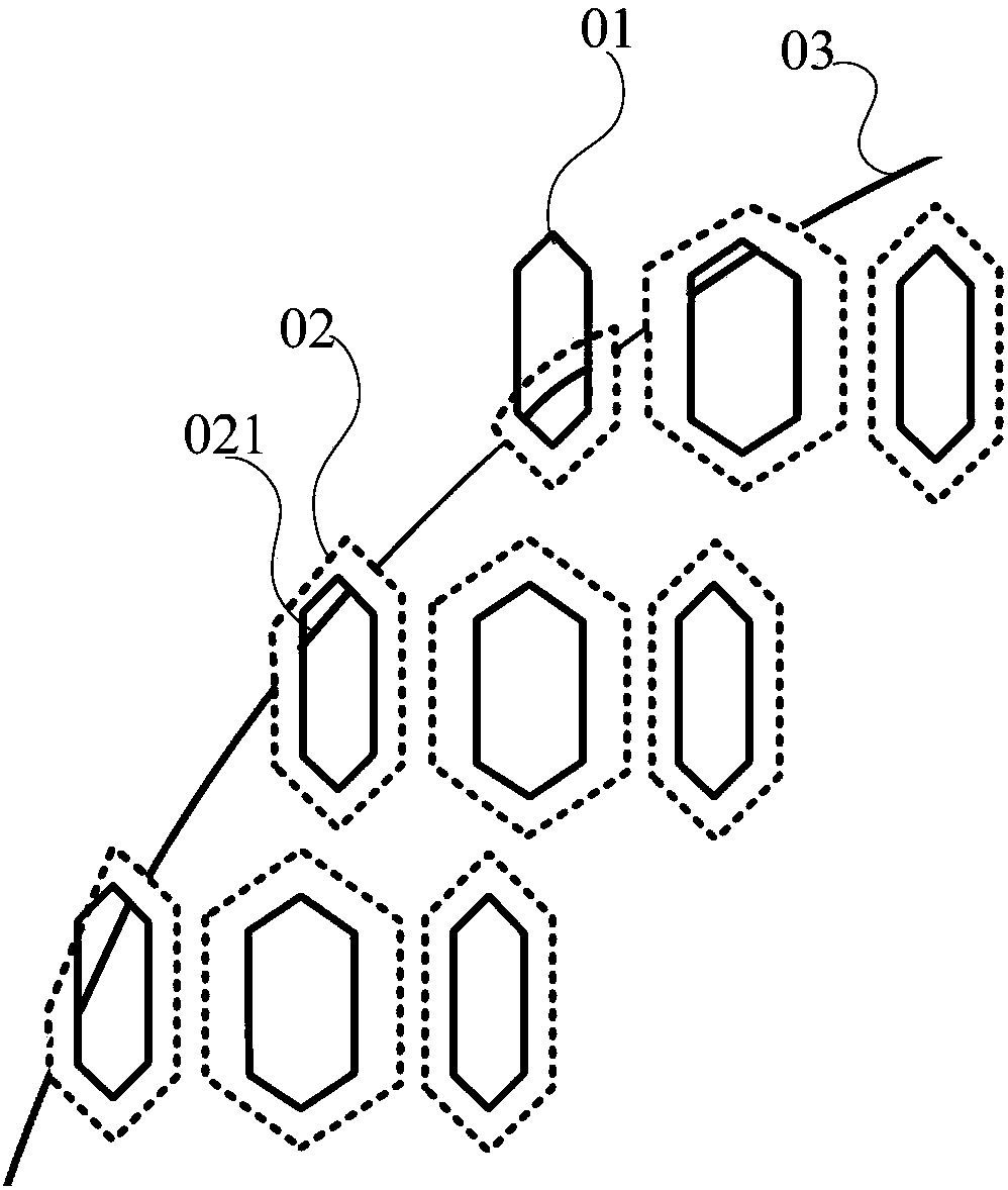
[0044] Specifically, such as figure 1 As shown, in the special-shaped display area, the opening area 01 of the pixel defining layer used to define the light emitting area of the sub-pixel is arranged in steps. figure 1 In the illustration, the shape of each opening area 01 is a hexagon surrounded by a solid line as an example. Correspondingly, the hollow area 021 of the FMM used to make the light-emitting functional layer 02 of the sub-pixel is consistent with the shape and size of the opening area 01 of the pixel definition layer, that is, the two overlap each other. Due to the shadow area (Shadow) in the evaporation process, the pattern of the final light-emitting functional layer 02 is larger than the hollow area 021 of the FMM. figure 1 The hexagon surrounded by dotted lines in the diagram indicates the pattern of the produced light-emitting functional layer 02 . Since the opening area 01 of the pixel definition layer is arranged in steps at the ideal edge 03 of the sp...
PUM
 Abstract
Description
Claims
Application Information
 - R&D
- Intellectual Property
- Life Sciences
- Materials
- Tech Scout
- Unparalleled Data Quality
- Higher Quality Content
- 60% Fewer Hallucinations
Browse by: Latest US Patents, China's latest patents, Technical Efficacy Thesaurus, Application Domain, Technology Topic, Popular Technical Reports.
© 2025 PatSnap. All rights reserved.Legal|Privacy policy|Modern Slavery Act Transparency Statement|Sitemap|About US| Contact US: help@patsnap.com


