an image sensor
An image sensor and sensor technology, which is applied in the field of exposure detection, can solve problems such as uneven backscattering in the photodiode array area, image sensors are easily blocked by objects to be measured, and unstable detection capabilities, so as to improve sensitivity and light utilization. , the effect of increasing the detection area
- Summary
- Abstract
- Description
- Claims
- Application Information
AI Technical Summary
Problems solved by technology
Method used
Image
Examples
Embodiment 1
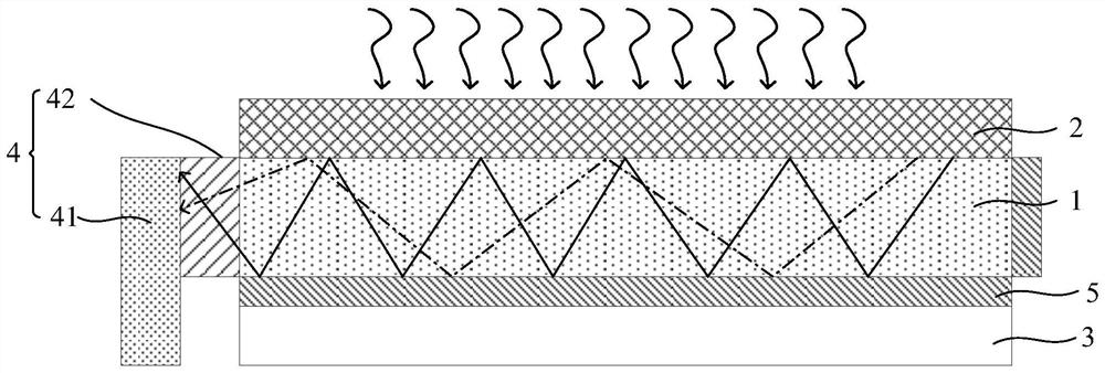
[0041] Such as image 3 As shown, this embodiment provides an image sensor, and the image sensor includes:
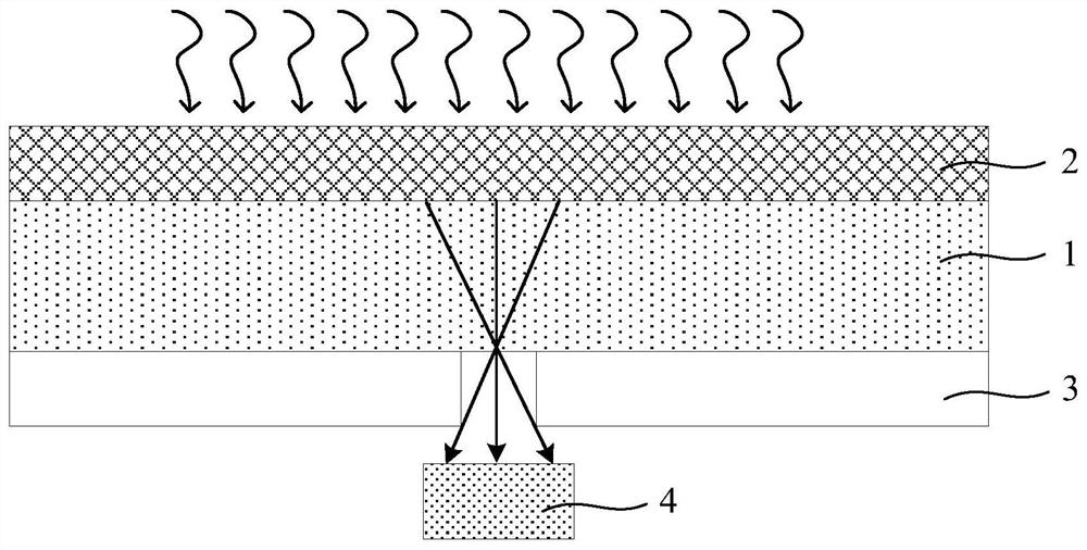
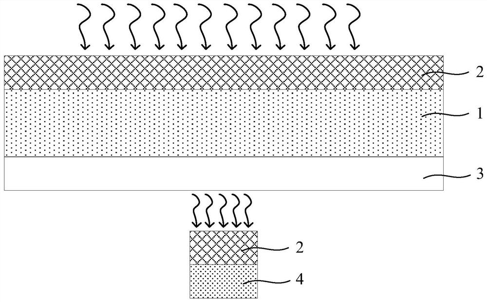
[0042] An array structure 1, the array structure 1 comprising a substrate, and an image sensor array located above the substrate;
[0043] a scintillator 2 located above the array structure 1;
[0044] A reflective layer 5 surrounding the array structure 1, wherein the reflective layer 5 is provided with at least one opening exposing the array structure 1;
[0045] an exposure detection structure 4 located at said opening; and
[0046] The backscattering layer 3 located below the reflective layer 5 .
[0047] Specifically, the substrate is a uniform transparent substrate, including one of sapphire or fused silica.
[0048] Specifically, the scintillator 2 is formed of a material with relatively high reflectivity; preferably, in this embodiment, the scintillator 2 includes gadolinium oxysulfide (GOS) or cesium iodide (CsI); of course, in In other embodiments, the sc...
Embodiment 2
[0061] like Figure 4 As shown, the difference between the image sensor of this embodiment and the image sensor described in Embodiment 1 is that the position of the opening on the reflective layer 5 and the position of the exposure detection structure 4 are different; the reflection path of visible light in the array structure 1 described in this embodiment like Figure 4 As shown, specifically, the visible light is captured by the exposure sensor through the optical adhesive layer 42 after multiple reflections, thereby realizing the exposure detection of the image sensor.
Embodiment 3
[0063] like Figure 5 As shown, the difference between the image sensor of this embodiment and the image sensor described in Embodiments 1 and 2 is that the position of the opening on the reflective layer 5 and the position of the exposure detection structure 4 are different; The reflection path of Figure 5 As shown, specifically, the visible light is captured by the exposure sensor through the optical adhesive layer 42 after multiple reflections, thereby realizing the exposure detection of the image sensor.
[0064] In summary, the image sensor of the present invention has the following beneficial effects:
[0065] 1. The image sensor of the present invention uses a scintillator and a reflective layer to construct the array structure into a light guide plate with better light guiding properties, which can guide the visible light generated by X-ray exposure at any position to the opening of the reflective layer, The influence of the image sensor being blocked by the shootin...
PUM
 Abstract
Description
Claims
Application Information
 - R&D
- Intellectual Property
- Life Sciences
- Materials
- Tech Scout
- Unparalleled Data Quality
- Higher Quality Content
- 60% Fewer Hallucinations
Browse by: Latest US Patents, China's latest patents, Technical Efficacy Thesaurus, Application Domain, Technology Topic, Popular Technical Reports.
© 2025 PatSnap. All rights reserved.Legal|Privacy policy|Modern Slavery Act Transparency Statement|Sitemap|About US| Contact US: help@patsnap.com


