Nonlinear material-based voltage-sharing electrode in basin type insulator
A nonlinear material, basin-type insulator technology, applied in insulators, circuits, electrical components, etc., can solve problems such as dwell simulation analysis
- Summary
- Abstract
- Description
- Claims
- Application Information
AI Technical Summary
Problems solved by technology
Method used
Image
Examples
Embodiment 1
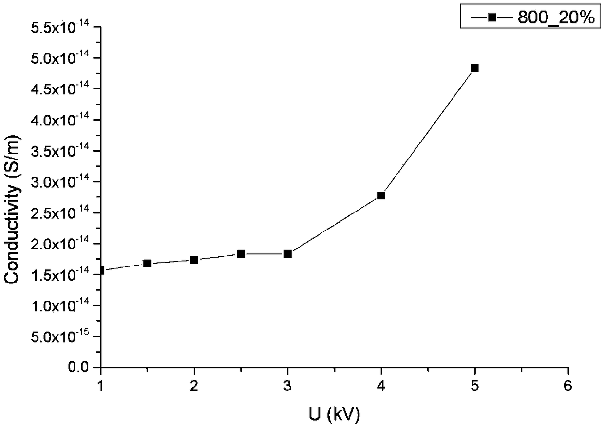
[0026] figure 2 It is a schematic diagram of the nonlinear coating resistivity of the voltage equalizing electrode in the pot insulator of the nonlinear material of the present invention changing with the electric field intensity, as figure 2 As shown, the epoxy coating modified by nonlinear material SiC is added to the surface of the central insert of the pot insulator. The coating has the characteristics of resistance nonlinearity, that is, the resistivity of the coating increases with the increase of the electric field intensity , and the rate of increase in resistivity increases. This feature enables a sharp drop in resistivity under high field strength, thereby realizing charge discharge under high field strength.
Embodiment 2
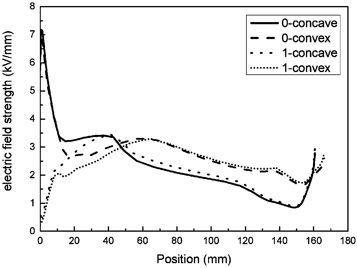
[0028] Apply a voltage of -300kV at the central electrode, image 3 is the electric field modulus distribution diagram of the present invention after applying -300kV voltage at the central electrode place, such as image 3 As shown, the electric field intensity near the embedded central electrode without surface coating is as high as 7kV / mm, while the electric field intensity near the embedded central electrode with surface coating is reduced to the level of 2kV / mm, which can largely Weaken the discharge phenomenon at the center electrode, thereby reducing the surface charge injected from the electrode.
Embodiment 3
[0030] Apply a voltage of -300kV at the central electrode, Figure 4 is the normal electric field modulus distribution diagram of the present invention after applying -300kV voltage at the central electrode; Figure 5 is the tangential electric field modulus distribution diagram of the present invention after applying a -300kV voltage at the central electrode, such as Figure 4 , Figure 5 As shown, the normal electric field strength is reduced from 6.5kV / mm to 2kV / mm, which can reduce the charge adsorption phenomenon on the surface of the pot insulator near the center electrode to a certain extent, thereby reducing the surface charge adsorbed from the space. The tangential electric field is basically unchanged, which can ensure that the surface flashover voltage of the pot insulator does not decrease under the condition of no charge accumulation.
PUM
 Abstract
Description
Claims
Application Information
 - R&D
- Intellectual Property
- Life Sciences
- Materials
- Tech Scout
- Unparalleled Data Quality
- Higher Quality Content
- 60% Fewer Hallucinations
Browse by: Latest US Patents, China's latest patents, Technical Efficacy Thesaurus, Application Domain, Technology Topic, Popular Technical Reports.
© 2025 PatSnap. All rights reserved.Legal|Privacy policy|Modern Slavery Act Transparency Statement|Sitemap|About US| Contact US: help@patsnap.com


