
Buffer device, manufacturing method of buffer device, backlight module, display device and manufacturing method of display device

A buffer device and backlight module technology, applied in optics, nonlinear optics, instruments, etc., can solve the problems of whitening and shining, light leakage, affecting the quality of display device products, etc., and achieve the effect of reducing impact and accurate alignment

Active Publication Date: 2018-08-03
BOE TECH GRP CO LTD +1
View PDF9 Cites 8 Cited by
  • Summary
  • Abstract
  • Description
  • Claims
  • Application Information

AI Technical Summary

Problems solved by technology

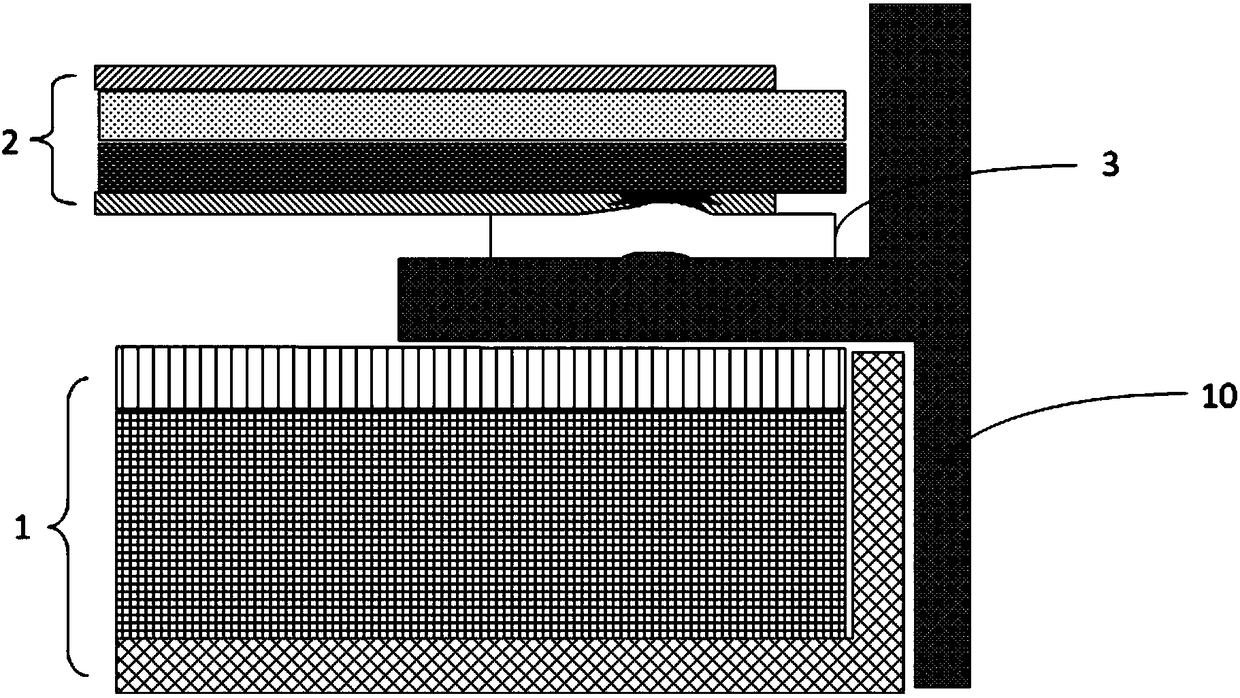
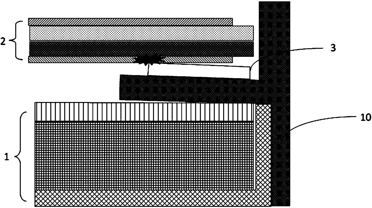
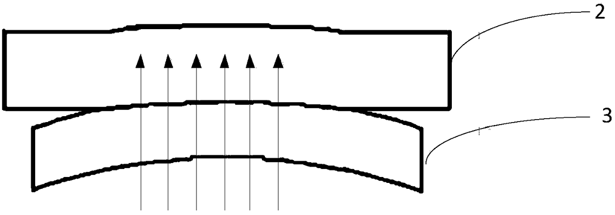
However, if image 3 and Figure 4 As shown, if the surface of the plastic frame of the backlight module 1 is uneven, it is easy for the buffer device 3 to exert a certain force on the display panel 2, causing the display panel 2 to generate stress. There will be a whitening and shining phenomenon in the area of ​​the force, thereby forming L0 light leakage; moreover, since the buffer device 3 is in contact with the surface of the display panel to form an adhesive layer, so that the display panel 2 and the backlight module 1 are not aligned properly without accurate alignment. When they are bonded together, the relative position between the display panel 2 and the backlight module 1 cannot be adjusted, so that the assembly of the display panel 2 and the backlight module 1 is offset, which affects the product quality of the display device

Method used


Image

  • Buffer device, manufacturing method of buffer device, backlight module, display device and manufacturing method of display device
  • Buffer device, manufacturing method of buffer device, backlight module, display device and manufacturing method of display device
  • Buffer device, manufacturing method of buffer device, backlight module, display device and manufacturing method of display device

Examples


Embodiment Construction

[0044] The following will clearly and completely describe the technical solutions in the embodiments of the present invention with reference to the accompanying drawings in the embodiments of the present invention. Obviously, the described embodiments are only some, not all, embodiments of the present invention. Based on the embodiments of the present invention, all other embodiments obtained by persons of ordinary skill in the art without creative efforts fall within the protection scope of the present invention.

[0045] see Figure 5-Figure 10 The buffer device 3 provided by the embodiment of the present invention includes a buffer body 30 and a hollow buffer layer 31 formed on the buffer body 30. The hollow buffer layer 31 includes a plurality of hollow parts 312 and a plurality of non-hollow parts 311; the buffer body 30 corresponds to the hollow An adhesive layer 300 is formed on the surface of the hollow portion 312 of the buffer layer 31 . It can be known that component...


PUM

PropertyMeasurementUnit
Thicknessaaaaaaaaaa

Abstract

The invention discloses a buffer device, a manufacturing method of the buffer device, a backlight module, a display device and a manufacturing method of the display device and relates to the technicalfield of display. On the premise that the assembly accuracy of a display panel and the backlight module is improved, the probability that foreign matter enters the display device is lowered, and theL0 light leakage phenomenon of the display device is reduced. The buffer device comprises a buffer body and a hollowed-out buffer layer which is formed on the buffer body, the hollowed-out buffer layer comprises multiple hollowed-out parts and multiple non-hollowed-out parts, and glue layers are formed on the surfaces, corresponding to the hollowed-out parts of the hollowed-out buffer layer, of the buffer body. The backlight module comprises the buffer device. The buffer device, the backlight module, the display device and the manufacturing method of the display device are applied to manufacturing of the display device.

Description

technical field [0001] The invention relates to the field of display technology, in particular to a buffer device and a manufacturing method thereof, a backlight module, a display device and a manufacturing method thereof. Background technique [0002] Liquid crystal display (Liquid Crystal Display, LCD) has the advantages of good picture quality, thin profile, low power consumption, etc., and is widely used in various fields such as mobile display, consumer communication or electronic products; such as figure 1 with figure 2 As shown, the existing liquid crystal display includes a backlight module 1 and a display panel 2 arranged on the light emitting surface of the backlight module. [0003] Among them, such as figure 1 with figure 2 As shown, a buffer device 3 is provided on the plastic frame of the backlight module 1 , and an adhesive layer is formed on the surface of the buffer device 3 contacting the display panel 2 to prevent foreign matter from entering the gap ...

Claims


Application Information

Patent Timeline
IPC IPC(8): G02F1/1333G02F1/13357
CPCG02F1/133308G02F1/133608G02F1/1336G02F2202/28G02F1/133311G02F1/133317G02F1/1303G02F1/133322G02F1/133325
Inventor 徐兵暴军萍郁信波金香馥
Owner BOE TECH GRP CO LTD
Learn More