Gate driving circuit, driving method thereof and display device
A gate drive circuit and drive group technology, applied to static indicators, static memory, instruments, etc., can solve problems such as display energy consumption
- Summary
- Abstract
- Description
- Claims
- Application Information
AI Technical Summary
Problems solved by technology
Method used
Image
Examples
Embodiment 1
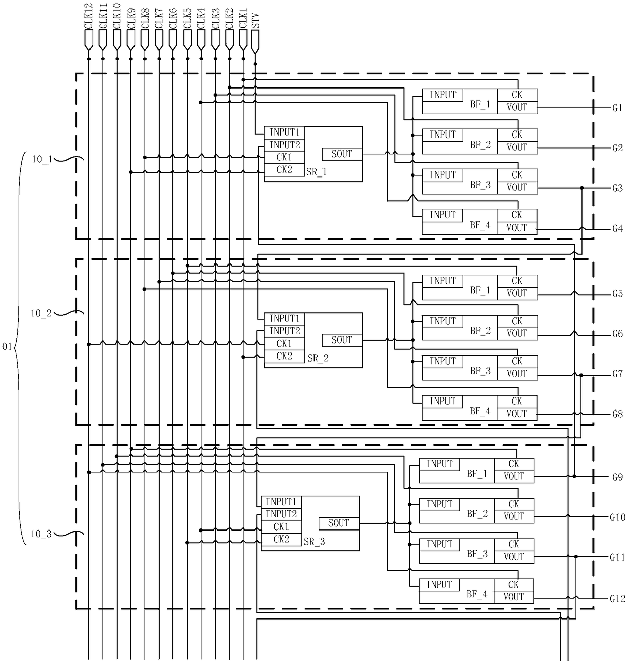
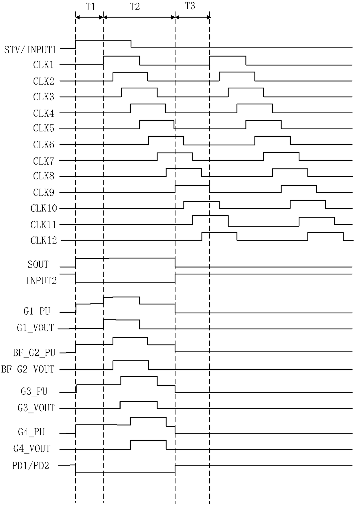
[0055] In this embodiment, the resolution that can be displayed by the display device with the above-mentioned gate driving circuit is an inherent resolution of 8K. In addition, the display device can also realize resolution conversion from 8K to 4K or conversion from 8K to 2K.
[0056] In this case, any one driving group 01 of the gate driving circuit is connected to 16 gate lines. Such as figure 2 Any one of the drive groups 01 shown above includes a first shift register unit 10_1 , a second shift register unit 10_2 , and a third shift register unit 10_3 cascaded in sequence.
[0057] Wherein, any shift register unit in the first shift register unit 10_1, the second shift register unit 10_2 and the third shift register unit 10_3 includes a first buffer subunit BF_1, a second buffer subunit BF_2, a third The buffer subunit BF_3 and the fourth buffer subunit BF_4.
[0058] In this case, the clock signal terminals CK of the first buffer subunit BF_1, the second buffer subuni...
Embodiment 2
[0075] In this embodiment, the display device having the above-mentioned gate driving circuit can realize the conversion of the resolution from the native resolution of 8K to 4K.
[0076] In this case, any one driving group 01 of the gate driving circuit is connected to 16 gate lines. Such as Figure 6 Any one of the drive groups 01 shown above includes a first shift register unit 10_1 , a second shift register unit 10_2 , a third shift register unit 10_3 and a fourth shift register unit 10_4 cascaded in sequence.
[0077] Wherein, any shift register unit in the first shift register unit 10_1, the second shift register unit 10_2, the third shift register unit 10_3 and the fourth shift register unit 10_4 includes the first buffer subunit BF_1, the second Two buffer subunits BF_2.
[0078] In this case, the clock signal terminals CK of the first buffer subunit BF_1 and the second buffer subunit BF_2 in the first shift register unit 10_1 are connected to the first system clock ...
PUM
 Abstract
Description
Claims
Application Information
 - R&D
- Intellectual Property
- Life Sciences
- Materials
- Tech Scout
- Unparalleled Data Quality
- Higher Quality Content
- 60% Fewer Hallucinations
Browse by: Latest US Patents, China's latest patents, Technical Efficacy Thesaurus, Application Domain, Technology Topic, Popular Technical Reports.
© 2025 PatSnap. All rights reserved.Legal|Privacy policy|Modern Slavery Act Transparency Statement|Sitemap|About US| Contact US: help@patsnap.com


