A green light organic electroluminescent device
An electroluminescence, electromechanical technology, applied in the field of organic electroluminescence devices, can solve the problems of high cost, high doping concentration, low energy of green OLED light-emitting layer, etc., to improve efficiency, improve device efficiency and life, improve excitation The effect of sub-utilization
- Summary
- Abstract
- Description
- Claims
- Application Information
AI Technical Summary
Problems solved by technology
Method used
Image

Examples
Embodiment 1
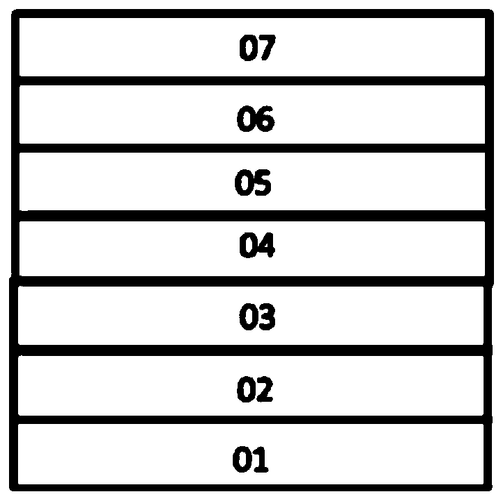
[0070] Such as image 3 As shown, a green light organic electroluminescent device provided by the present invention includes a substrate, and a first electrode layer 01, a light emitting layer 04, and a second electrode layer 07 sequentially formed on the substrate. The first electrode A first organic functional layer is arranged between the layer 01 and the light-emitting layer 04, and a second organic functional layer is arranged between the light-emitting layer 04 and the second electrode layer 07. The first organic functional layer is a hole injection layer 02 and / or a hole transport layer 03, and the second organic functional layer is an electron transport layer 05 and / or an electron injection layer 06.
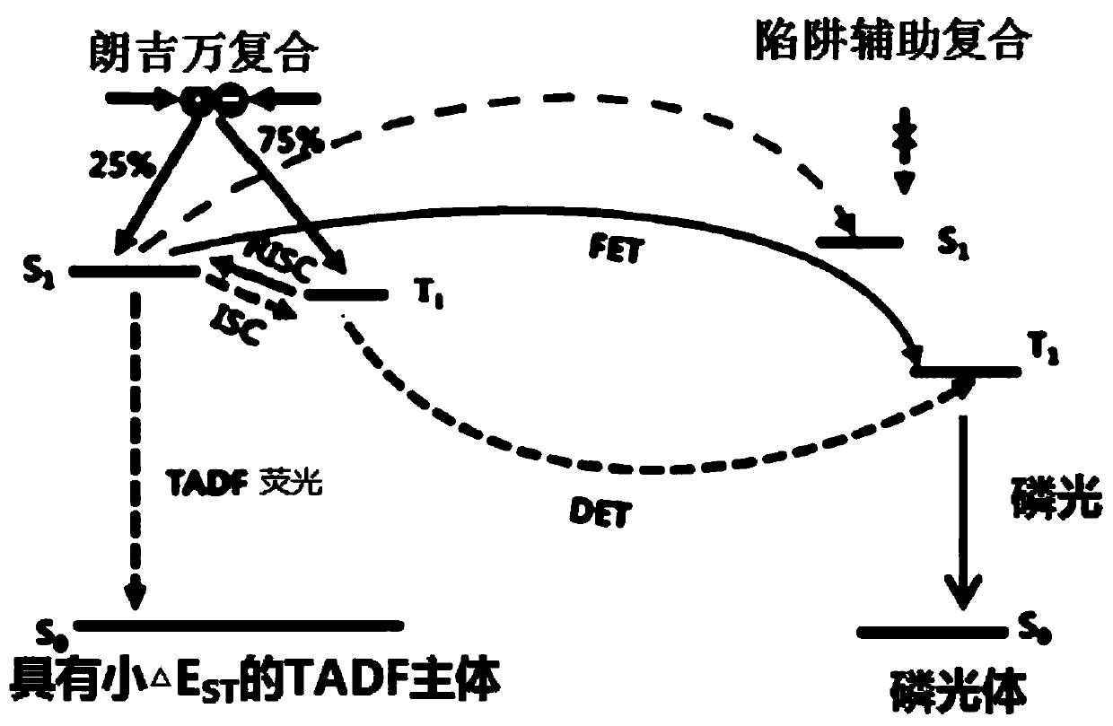
[0071] The light-emitting host materials of the device of this embodiment are thermally activated delayed fluorescent materials and hole-type transport materials doped or not doped with hole-type transport materials, and the mass ratio of the thermally activated delayed fluo...
Embodiment 2
[0081] The light-emitting devices of device 2 to device 5 have the same structure as the light-emitting device of device 1, except that the doping concentration of the green phosphorescent dye is different. Its structure is as follows:
[0082] ITO / NPB(40nm) / TCTA(10nm) / Formula 2-1: 0.5~5wt% Ir(ppy) 2 (acac)(20nm) / Bp hen(40nm) / LiF(5nm) / Al
[0083] Table 3 Performance test results of device 2 to device 5
[0084]
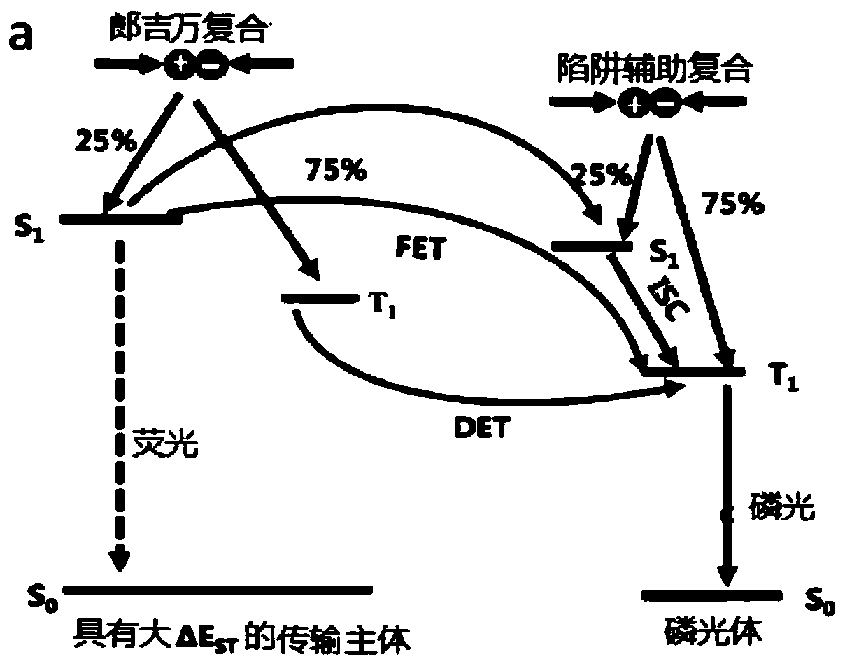
[0085] The performance of the light-emitting device of device 2 to device 5 was tested, as shown in Table 3, at 5000cd / m 2 Under brightness, as the doping concentration of the dye increases, the current efficiency of the device also increases. This is because the long-range Energy transfer improves the exciton utilization rate, which in turn improves the device efficiency.
Embodiment 3
[0087] The light-emitting devices of devices 6 to 10 have the same structure as the light-emitting device of Example 1, except that the host material of the light-emitting layer 06 is different. Its structure is as follows:
[0088] ITO / NPB(40nm) / TCTA(10nm) / host material: 3wt% Ir(ppy) 2 (acac)(20nm) / Bp hen(40nm) / LiF(5nm) / Al
[0089] Table 4 Performance test results of device 6 to device 10
[0090]
[0091] The performance of the light-emitting device from device 6 to device 10 is tested, as shown in Table 4, at 5000cd / m 2 Under brightness, different thermally activated delayed fluorescent materials and different hole-type transport materials are co-evaporated. Although the doping ratio is different, the device performance shows low driving voltage and high efficiency, indicating the thermal activation delay protected by the present invention Fluorescence: The host material composed of hole-type transport materials has universality, and its devices have high-efficiency performance a...
PUM
| Property | Measurement | Unit |
|---|---|---|
| thickness | aaaaa | aaaaa |
Abstract
Description
Claims
Application Information
 - R&D
- Intellectual Property
- Life Sciences
- Materials
- Tech Scout
- Unparalleled Data Quality
- Higher Quality Content
- 60% Fewer Hallucinations
Browse by: Latest US Patents, China's latest patents, Technical Efficacy Thesaurus, Application Domain, Technology Topic, Popular Technical Reports.
© 2025 PatSnap. All rights reserved.Legal|Privacy policy|Modern Slavery Act Transparency Statement|Sitemap|About US| Contact US: help@patsnap.com