Buffering of fcob chips in a chip transfer device

A transfer device and chip technology, applied in transportation and packaging, semiconductor devices, electrical components, etc., can solve the problems of reducing assembly efficiency, uneven utilization, reducing the number of COB or FCOB chips, etc., and achieve the effect of low price

Active Publication Date: 2018-03-30
ASM ASSEMBLY SYST GMBH & CO
View PDF5 Cites 1 Cited by
  • Summary
  • Abstract
  • Description
  • Claims
  • Application Information

AI Technical Summary

Problems solved by technology

This uneven utilization reduces the effective assembly efficiency, that is, reduces the number of COB or FCOB chips that can be assembled within a pre-set time period

Method used


Image

  • Buffering of fcob chips in a chip transfer device
  • Buffering of fcob chips in a chip transfer device
  • Buffering of fcob chips in a chip transfer device

Examples


Embodiment Construction

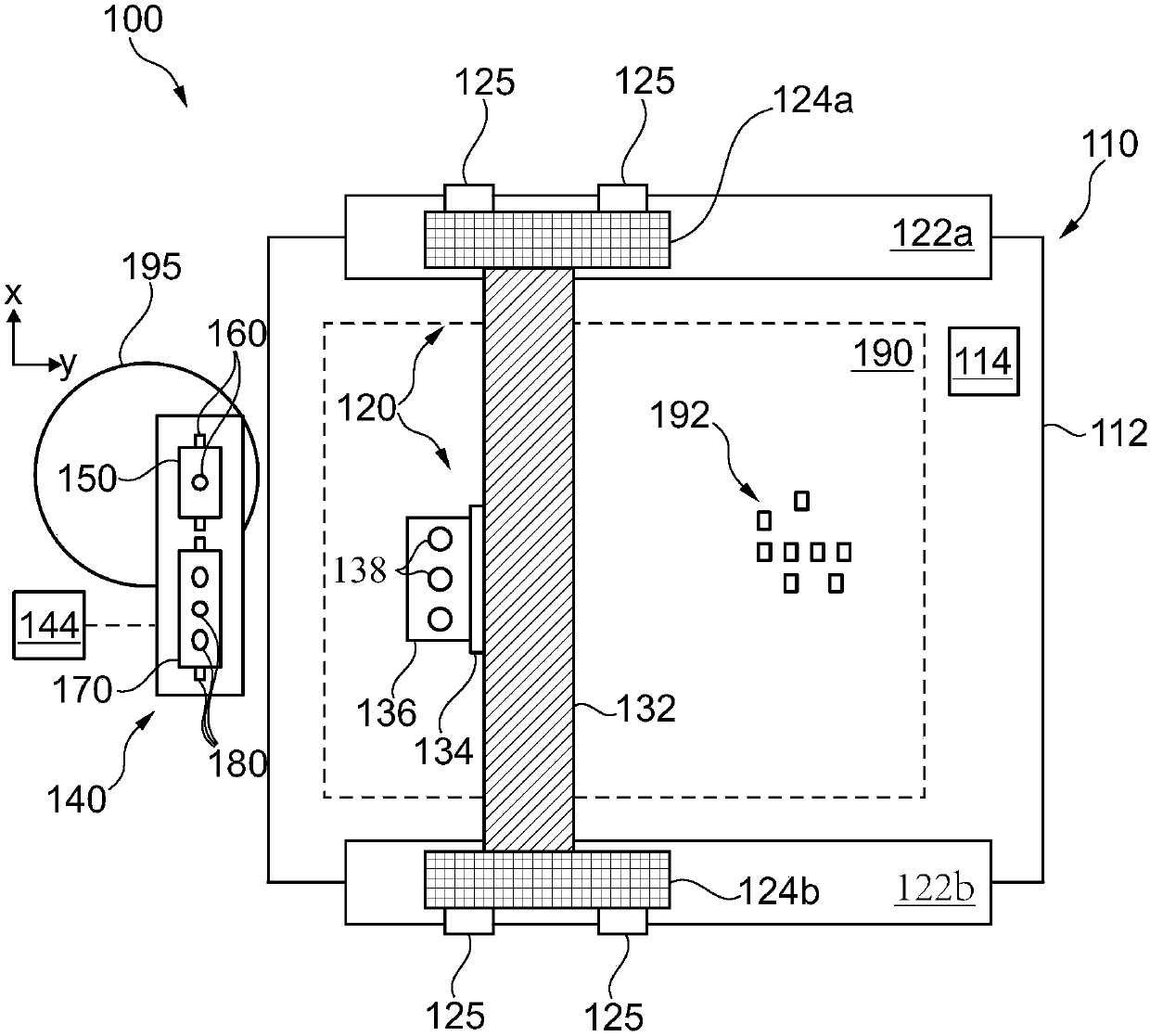
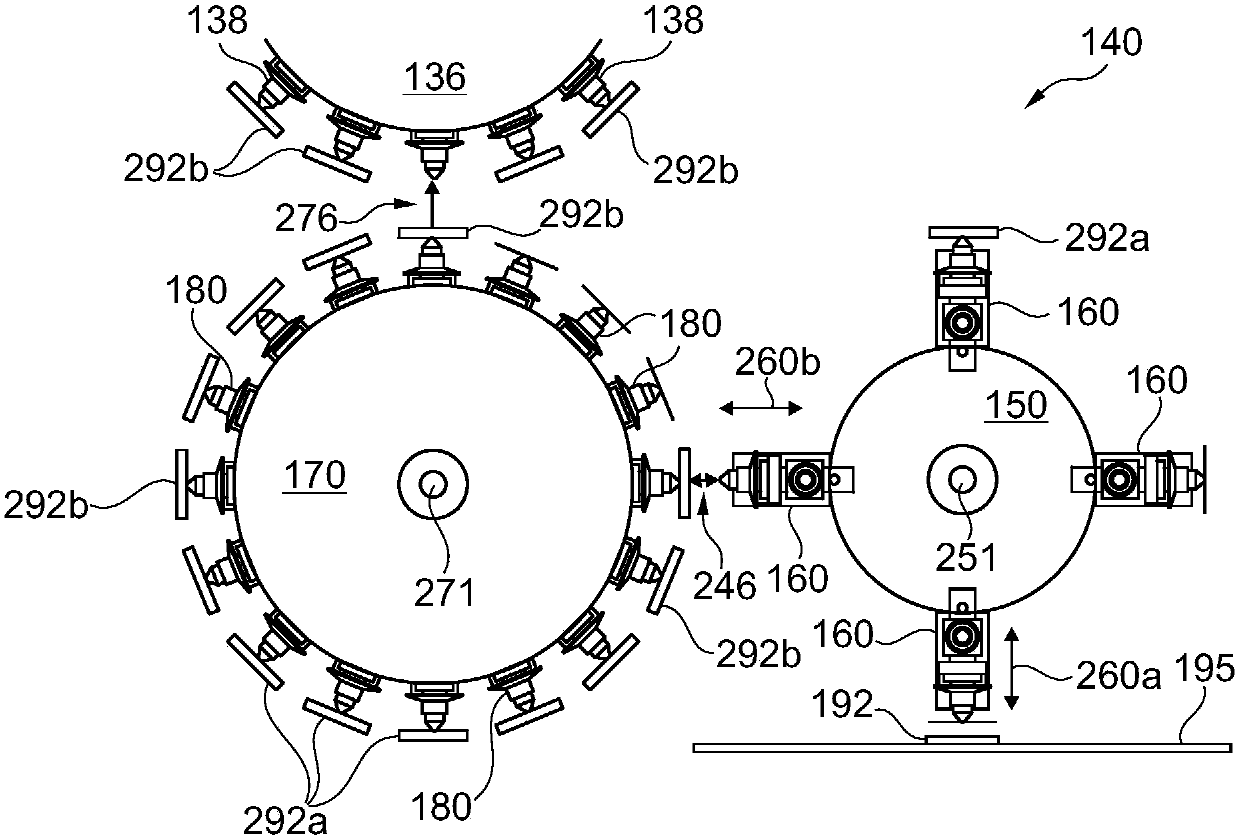
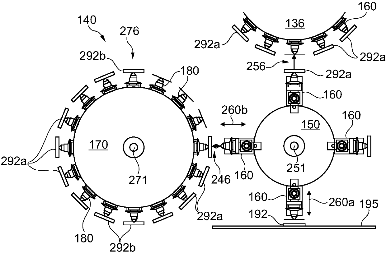
[0113] It should be noted that in the detailed description below, features or components of different embodiments (which are identical or at least functionally identical to corresponding features or components of other embodiments) are provided with the same reference signs or different reference signs. The last two letters are the same as reference numbers for features or components that are identical or at least functionally identical. In order to avoid unnecessary repetition, features or components which have already been explained with reference to the exemplary embodiments described above will not be explained in more detail below.

[0114] Furthermore, it should be pointed out that the embodiments described below are only selected from among the possible embodiments of the invention. In particular, it is possible to combine features of the individual exemplary embodiments with one another in a suitable manner, so that a multiplicity of different exemplary embodiments can...


PUM


Abstract

The invention provides a method for transferring a chip from a wafer to an assembling head of an automatic assembling machine, wherein the chip is overturned once at a first extracting position relative to an original position in the wafer, or is overturned twice at a second extracting position and is supplied to the assembling head. The method comprises the steps of taking the chip out of the wafer by means of a rotatable taking-out tool; rotating the taking-out tool so that the chip is arranged at a handover position, and transferring the chip from the taking-out tool to a rotatable storingtool. If the chip which is called as the FCOB chip is overturned once and is transferred to the assembling head, the method further comprises steps of transferring the FCOB chip from the storing toolback to the taking-out tool; re-rotating the taking-out tool so that the FCOB chip is arranged at the first extracting position; and receiving the re-rotated FCOB chip at the first extracting positionby the assembling head. Furthermore the invention describes a chip transfer device for executing method, and an assembling system with the chip transfer device.

Description

technical field [0001] The present invention relates to the technical field of assembling electronic components to component carriers, in particular to assembling component carriers with housingless electronic components constituted as chips, which are taken directly from the prepared wafer and supplied to the assembly craft. The invention relates in particular to a method for transferring chips from a wafer to a mounting head of an automatic assembly machine, as well as to a chip-transfer device for carrying out said method and to an assembly with an automatic assembly machine and such a chip-transfer device system. Background technique [0002] In order to achieve a high degree of integration of electronic components in an efficient manner, it is known to remove the electronic components in the form of chips directly from the wafer and place them on component carriers to be assembled by means of a mounting head of an automatic mounting machine. In terms of its original o...

Claims


Application Information

Patent Timeline
IPC IPC(8): H01L21/677H01L21/683
CPCH01L21/67718H01L21/6838H01L21/50H01L24/75H01L2224/75611H01L2224/75601H01L2224/75621H01L2224/75651H01L2224/75901H01L21/67721H01L21/67712H01L21/67144H01L21/67121
Inventor 罗美尔·塞巴斯蒂安罗斯曼·托马斯特里贾尼·米歇尔
Owner ASM ASSEMBLY SYST GMBH & CO
Why Eureka
Try Eureka