Sensor, driving method of sensor, OLED device and display device

A driving method and sensor technology, which are applied in the manufacturing of semiconductor devices, electric solid-state devices, and semiconductor/solid-state devices, etc., can solve the problems of complex driving current schemes, and achieve the effect of simplifying the driving current process and simple operation.

Active Publication Date: 2018-03-20
HEFEI XINSHENG OPTOELECTRONICS TECH CO LTD +1
View PDF12 Cites 0 Cited by
  • Summary
  • Abstract
  • Description
  • Claims
  • Application Information

AI Technical Summary

Problems solved by technology

[0003] However, in the prior art, the scheme of changing the driving current is more complicated

Method used


Image

  • Sensor, driving method of sensor, OLED device and display device
  • Sensor, driving method of sensor, OLED device and display device
  • Sensor, driving method of sensor, OLED device and display device

Examples


Embodiment Construction

[0026] In order for those skilled in the art to better understand the technical solution of the present invention, the sensor and its driving method, OLED device and display device provided by the present invention will be described in detail below with reference to the accompanying drawings.

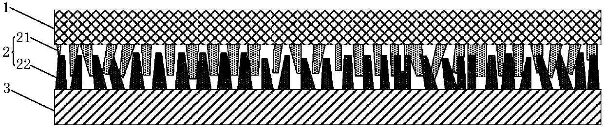
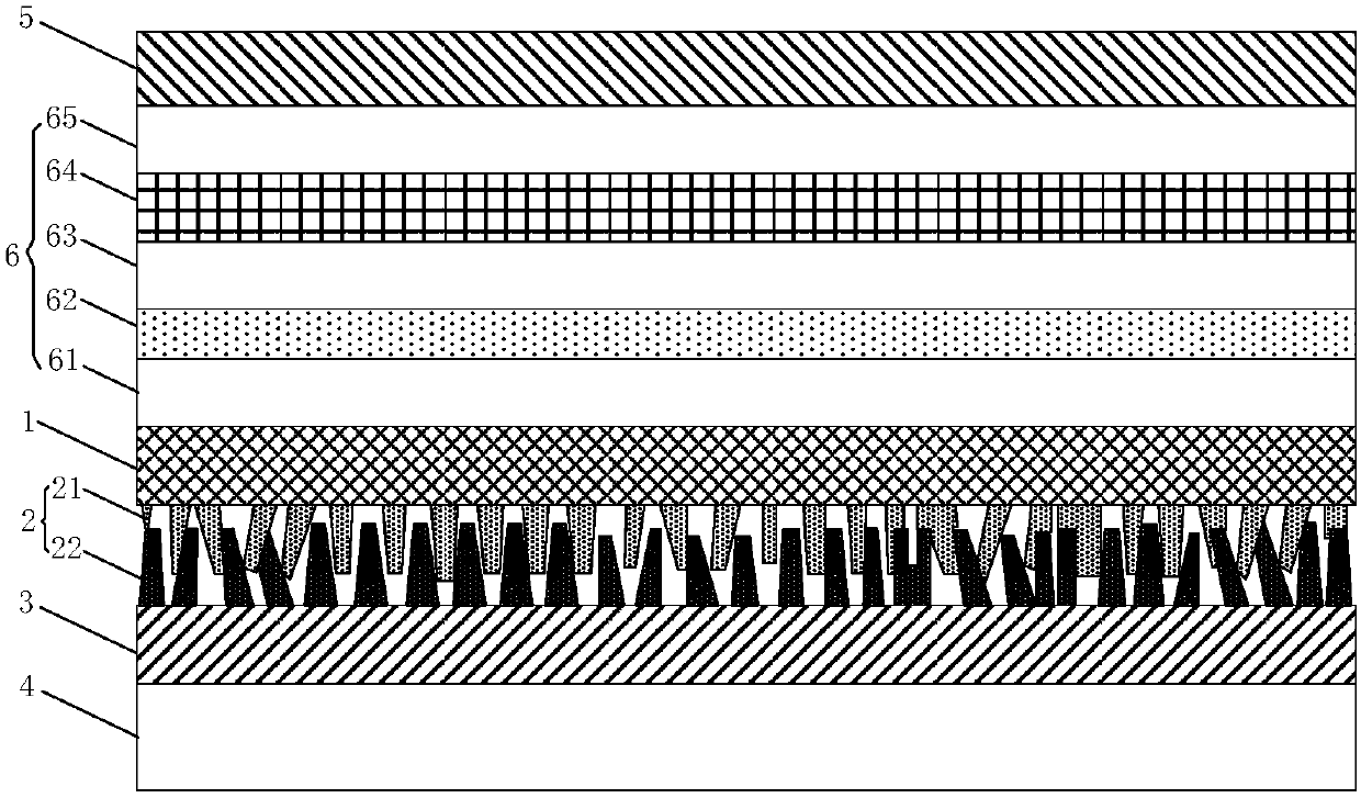
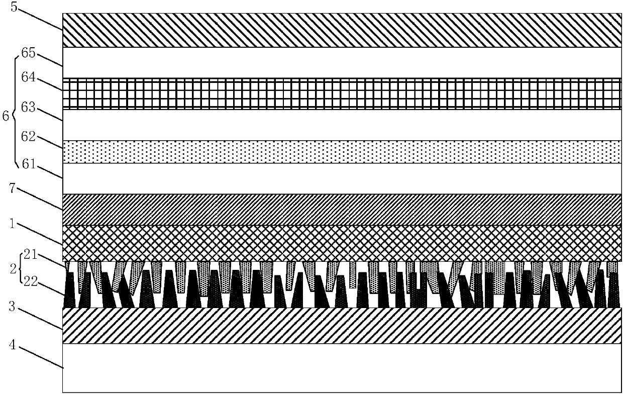
[0027] figure 1 A schematic structural diagram of a sensor provided in Embodiment 1 of the present invention, such as figure 1 As shown, the sensor includes a conductive layer 1, a contact layer 2 and an expansion layer 3, the contact layer 2 is located between the conductive layer 1 and the expansion layer 3, the contact layer 2 includes a first contact structure 21 and a second contact structure 22, the first The contact structure 21 is located on the conductive layer 1 , and the second contact structure 22 is located on the expansion layer 3 .

[0028] The expansion layer 3 serves to increase the contact area between the first contact structure 21 and the second contact structure 22...


PUM


Abstract

The invention discloses a sensor, a driving method of the sensor, an OLED device and a display device. The sensor comprises a conductive layer, a contact layer and an expansion layer. The contact layer is located between the conductive layer and the expansion layer. The contact layer comprises a first contact structure and a second contact structure. The first contact structure is located on the conductive layer. The second contact structure is located on the expansion layer. The expansion layer is used for increasing the contact area between the first contact structure and the second contactstructure during the expansion process. Or, the expansion layer is used for reducing the contact area between the first contact structure and the second contact structure during the contraction process. According to the invention, the driving current of the OLED device is changed by expanding or contracting the expansion layer. The operation is simple, and the scheme for changing the driving current of the OLED device is simplified.

Description

technical field [0001] The invention relates to the field of display technology, in particular to a sensor and a driving method thereof, an OLED device and a display device. Background technique [0002] Organic light-emitting diode (Organic Light-Emitting Diode, referred to as: OLED) is an electroluminescent device, which has the characteristics of self-luminescence, high luminous efficiency, low operating voltage, light and thin, flexible and simple process technology, and is used in display lighting and other fields. more extensive. In the existing OLED devices, the change of the driving current of the OLED device is mainly realized by changing the driving voltage of the device. [0003] However, in the prior art, the scheme of changing the driving current is relatively complicated. Contents of the invention [0004] The invention provides a sensor and its driving method, an OLED device and a display device, which are used for simplifying the scheme of changing the dr...

Claims


Application Information

Patent Timeline
Patent Type & Authority Applications(China)
IPC IPC(8): G09G3/3241H01L51/52
CPCG09G3/3241H10K50/80
Inventor 王欣欣贾文斌彭锐
Owner HEFEI XINSHENG OPTOELECTRONICS TECH CO LTD
Why Eureka
Try Eureka