
Optimization method for temperature cyclic stress acceleration model of semiconductor device

A cyclic stress and acceleration model technology, which is applied in instruments, special data processing applications, electrical digital data processing, etc., can solve the problem of inability to quickly and accurately select the temperature cyclic stress acceleration model, and achieve the effect of solving irrationality

Inactive Publication Date: 2018-02-16
NO 24 RES INST OF CETC
View PDF5 Cites 6 Cited by
  • Summary
  • Abstract
  • Description
  • Claims
  • Application Information

AI Technical Summary

Problems solved by technology

[0006] In view of this, the object of the present invention is to provide a method for optimizing the temperature cycle stress acceleration model of a semiconductor device, which can effectively select the optimal temperature cycle stress acceleration model suitable for this type of device, and quickly select this type of semiconductor device for subsequent use The optimal temperature cycle stress acceleration model provides a reference basis, which overcomes the problem that the temperature cycle stress acceleration model cannot be quickly and accurately selected when evaluating the storage life of the circuit

Method used


Image

  • Optimization method for temperature cyclic stress acceleration model of semiconductor device
  • Optimization method for temperature cyclic stress acceleration model of semiconductor device
  • Optimization method for temperature cyclic stress acceleration model of semiconductor device

Examples


Embodiment Construction

[0032] The preferred embodiments of the present invention will be described in detail below with reference to the accompanying drawings.

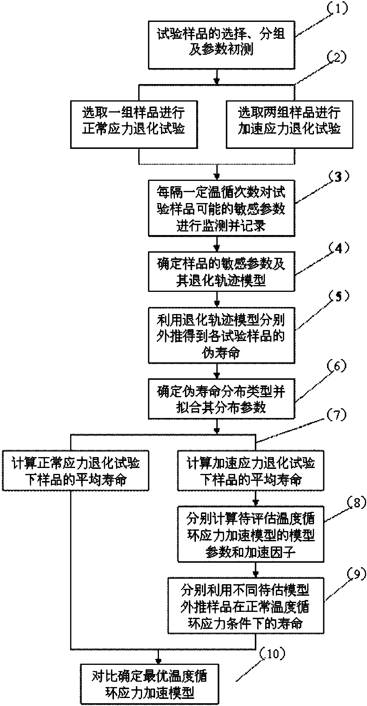
[0033] figure 1 It is a flow chart of the preferred method for the temperature cycle stress acceleration model of the semiconductor device of the present invention. Such as figure 1 As shown, the steps of the method for optimizing the temperature cycle stress acceleration model of a semiconductor device according to an embodiment of the present invention include:

[0034] Step (1): Randomly select ≥150 circuit samples from the qualified semiconductor devices, number each device sample, conduct a full-parameter test on each device sample according to the detailed product specification, and record all the circuit samples of the tested device sample. Parameter value, randomly divided into 3 groups (each group ≥ 50);

[0035] Step (2): Randomly select one group of device samples, and conduct a degradation test under normal temperature cycle ...


PUM


Abstract

The invention discloses an optimization method for a temperature cyclic stress acceleration model of a semiconductor device, and belongs to the field of integrated circuits. The method comprises the steps of performing a normal stress degradation test on a group of samples by utilizing a cyclic stress, and performing an accelerated degradation test on another two groups of samples by utilizing anincreased constant temperature cyclic accelerated stress; performing detection and determination on sample sensitive parameters every a certain temperature cyclic frequency, obtaining a degradation path model, obtaining a pseudo-life and a distribution type, and performing fitting to obtain distribution parameters; calculating average lives of the samples in the normal stress degradation test andthe accelerated stress test, and calculating model parameters and acceleration factors of a to-be-assessed temperature cyclic stress acceleration model; and inferring the lives of the samples in a normal cyclic stress condition, and performing comparison with sample lives obtained by performing extrapolation through adopting different to-be-assessed stress acceleration models, wherein the model with an optimal life value is an optimal model. According to the method, the optimal temperature cyclic stress acceleration model can be accurately judged.

Description

technical field [0001] The invention belongs to the field of integrated circuits and relates to a method for optimizing a temperature cycle stress acceleration model of a semiconductor device. Background technique [0002] Existing long-life evaluation tests for analog integrated circuits include two evaluation methods: accelerated life testing (Accelerated Life Testing, ALT) and accelerated degradation testing (Accelerated Degradation Testing, ADT). Although the research history of accelerated life test evaluation methods is long, and the processing of relevant life data is relatively easy. However, the accelerated stress test for high-reliability and long-life analog integrated circuits often results in very few failures or no failures at all, so it is necessary to obtain sufficient failure data by increasing the number of samples or increasing the test time, which makes the test cost And the test cycle is unbearable. [0003] The accelerated degradation test is to accel...

Claims


Application Information

Patent Timeline
IPC IPC(8): G06F17/50
CPCG06F30/367G06F2119/04G06F2119/08
Inventor 吴兆希罗俊邱忠文
Owner NO 24 RES INST OF CETC
Learn More