A kind of preparation method of curved surface hydrophobic microstructure
A technology of microstructure and curved surface is applied in the field of preparation of curved surface hydrophobic microstructure, which can solve the problems of high cost, lack of scale, low-cost preparation capability, etc., and achieves the effect of simple process, low material cost, and improved preparation method.
- Summary
- Abstract
- Description
- Claims
- Application Information
AI Technical Summary
Problems solved by technology
Method used
Image
Examples
Embodiment 1
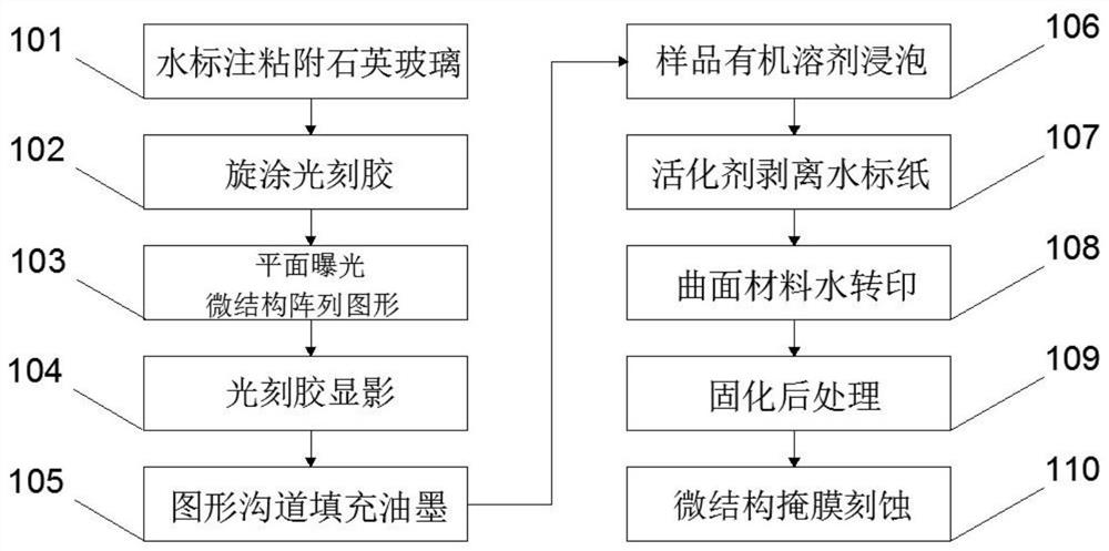
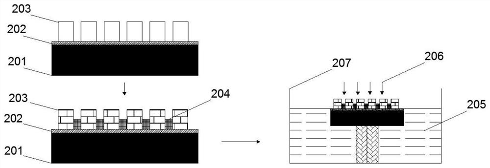
[0038] The first step 101: Adhere the peelable water mark paper on the quartz glass, use a 4-12 inch semiconductor quartz glass sheet 201, and use resin to bond the peelable water mark paper 202. The size of the water mark paper is the same as that of the quartz glass sheet. same size.
[0039] The second step 102: Coat the photoresist 203 on the water mark paper and cure it. Use a photoresist spin coater to coat the photoresist to ensure a thickness of 30-80 microns. The thermal curing time is determined by the specific material and thickness. In this example, a positive photoresist with a thickness of 30 microns is used, and the curing time is about 15 minutes.
[0040] The third step 103: use a plane exposure machine to complete the exposure of the microstructure pattern. The microstructure pattern is an array pattern formed by repeated arrangement of a single pattern, and the pattern is one of square, circle and regular hexagon. In this example, a square pattern is used. ...
Embodiment 2
[0048] The first step 101: Adhere the peelable water mark paper 202 on the quartz glass, use a 4-12 inch semiconductor quartz glass sheet 201, and use resin to bond the peelable water mark paper. The size of the water mark paper is the same as that of the quartz glass sheet. same size.
[0049] The second step 102: Coat the photoresist 203 on the water mark paper and cure it. Use a photoresist spin coater to coat the photoresist to ensure a thickness of 30-80 microns. The thermal curing time is determined by the specific material and thickness. In this example, a positive photoresist with a thickness of 40 microns is used, and the curing time is about 25 minutes.
[0050] The third step 103: use a plane exposure machine to complete the exposure of the microstructure pattern. The microstructure pattern is an array pattern formed by repeated arrangement of a single pattern, and the pattern is one of square, circle and regular hexagon. In this example, a square pattern is used. ...
PUM
| Property | Measurement | Unit |
|---|---|---|
| diameter | aaaaa | aaaaa |
| height | aaaaa | aaaaa |
| depth | aaaaa | aaaaa |
Abstract
Description
Claims
Application Information
 - Generate Ideas
- Intellectual Property
- Life Sciences
- Materials
- Tech Scout
- Unparalleled Data Quality
- Higher Quality Content
- 60% Fewer Hallucinations
Browse by: Latest US Patents, China's latest patents, Technical Efficacy Thesaurus, Application Domain, Technology Topic, Popular Technical Reports.
© 2025 PatSnap. All rights reserved.Legal|Privacy policy|Modern Slavery Act Transparency Statement|Sitemap|About US| Contact US: help@patsnap.com


