
Metal gate preparation method for 3D NAND memory device

A memory and metal gate technology, which is applied in semiconductor/solid-state device manufacturing, electric solid-state devices, semiconductor devices, etc., can solve the problems of narrowing openings, etc., and achieve increased size, good lateral filling performance of metal gates, and smooth diffusion channels. Effect

Inactive Publication Date: 2017-12-29
YANGTZE MEMORY TECH CO LTD
View PDF4 Cites 3 Cited by
  • Summary
  • Abstract
  • Description
  • Claims
  • Application Information

AI Technical Summary

Problems solved by technology

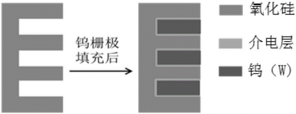
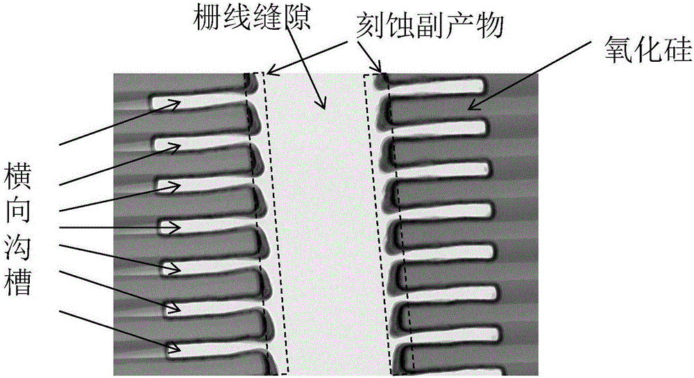
from the figure 2 It can be clearly seen that the etching byproducts (the part shown in the dotted box) accumulate at the opening of the trench, resulting in narrowing of the opening

Method used


Image

  • Metal gate preparation method for 3D NAND memory device
  • Metal gate preparation method for 3D NAND memory device
  • Metal gate preparation method for 3D NAND memory device

Examples


Embodiment Construction

[0034] The present invention is described in detail in conjunction with schematic diagrams. When describing the embodiments of the present invention in detail, for the convenience of explanation, the cross-sectional view showing the device structure will not be partially enlarged according to the general scale, and the schematic diagram is only an example, which should not limit the present invention. scope of protection. In addition, the three-dimensional space dimensions of length, width and depth should be included in actual production.

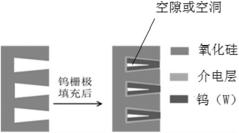
[0035] In the existing 3D NAND storage device manufacturing process, metal needs to be filled, and the lateral groove array forming the metal gate is formed by liquid phase chemical etching, and the etching by-products will be deposited at the opening of the groove during the process of backflow and removal. The oxide structure retained after liquid-phase chemical etching is in the shape of a "match head", which narrows the opening of the ...


PUM


Abstract

The embodiment of the invention provides a metal gate preparation method for a 3D NAND memory device, and the method comprises the steps: removing etching by-products which are generated in the liquid phase chemical etching of silicon nitride and are gathered at the opening of a lateral trench array before removing a silicon nitride layer in a stacked structure through a liquid phase chemical etching method and before filling each lateral trench of the lateral trench array with metal mediums. Because the etching by-products gathered at the opening of the lateral trench array is removed, the size of the trench opening is increased, and a smooth diffusion channel for the reaction gas in a subsequent metal gate filling process is provided, thereby preventing the lateral trenches from being sealed in advanced in the metal gate filling process, enabling reaction gas to be continuously let in a deep part of a structure for reaction deposition, and obtaining the good metal gate lateral filling performances.

Description

technical field [0001] The present application relates to the technical field of semiconductor processing, in particular to a method for preparing a metal gate of a 3D NAND storage device. Background technique [0002] The vertical storage structure of the existing 3D NAND storage device is formed by stacking multi-layer dielectric films. During the preparation process, the silicon nitride in the silicon oxide / silicon nitride alternate stacking structure needs to be removed to form a lateral trench array, and then Each lateral groove of the lateral groove array is filled with a metal medium, thereby forming a metal gate. [0003] In the process of filling the metal dielectric, the reaction gas needs to enter the trench array through completely parallel narrow diffusion channels and deposit a film on its sidewall (such as figure 1 As shown), therefore, the aspect ratio of the filled trench structure, the size of the key dimension and the uniformity of the structure have an i...

Claims


Application Information

Patent Timeline
Patent Type & Authority Applications(China)
IPC IPC(8): H01L21/02H01L27/11524H01L27/11551H01L27/1157H01L27/11578H10B41/20H10B41/35H10B43/20H10B43/35
CPCH01L21/02068H10B41/20H10B41/35H10B43/20H10B43/35
Inventor 唐浩左明光李远彭浩许爱春万先进
Owner YANGTZE MEMORY TECH CO LTD
Learn More