Adaptive asymmetric pin type chip drawing method
An asymmetric and self-adaptive technology, applied in printed circuit manufacturing, circuit board tool positioning, electrical components, etc., can solve the problem that the accuracy of chip parameter information cannot be directly observed
- Summary
- Abstract
- Description
- Claims
- Application Information
AI Technical Summary
Problems solved by technology
Method used
Image

Examples
specific Embodiment approach 1
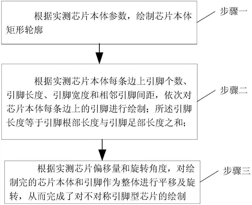
[0026] Specific implementation mode one: see figure 1 Describe this embodiment, a method for drawing an adaptive asymmetric pin type chip described in this embodiment, the method includes the following steps:
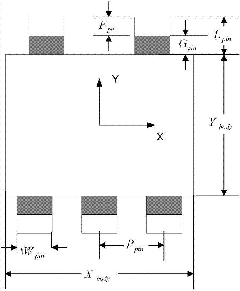
[0027] Step 1: Draw the rectangular outline of the chip body according to the measured chip body parameters. At this time, the position of the chip body defaults to the initial position; the measured chip body parameters include the dimension X of the rectangular profile in the X-axis direction. body and Y axis dimension Y body ; The length direction of the rectangular profile is the X-axis direction, and the width direction is the Y-axis direction;
[0028] Step 2: Draw the pins on each side of the chip body in turn according to the number of pins on each side of the chip body, the length of the pins, the width of the pins, and the distance between adjacent pins; the length of the pins is equal to The sum of the length of the root of the pin and the length of the foo...
specific Embodiment approach 2
[0032] Specific implementation mode two: see figure 1 This embodiment is described. The difference between this embodiment and the method for drawing an adaptive asymmetric pin-type chip described in the first embodiment is that the method of drawing the rectangular outline of the chip body according to the actual measured chip body parameters The specific process is as follows: according to the parameters of the chip body, the openGL graphics program interface function is used to draw a closed line segment, so as to obtain the rectangular outline of the chip body.
specific Embodiment approach 3
[0033] Specific implementation mode three: see figure 1 and figure 2 Describe this embodiment, the difference between this embodiment and the drawing method of an adaptive asymmetric pin type chip described in the first embodiment is that in the second step, according to the actual measurement of the pins on each side of the chip body The specific process of drawing the pins on each side of the chip body in order of number, pin length, pin width and adjacent pin spacing is as follows:
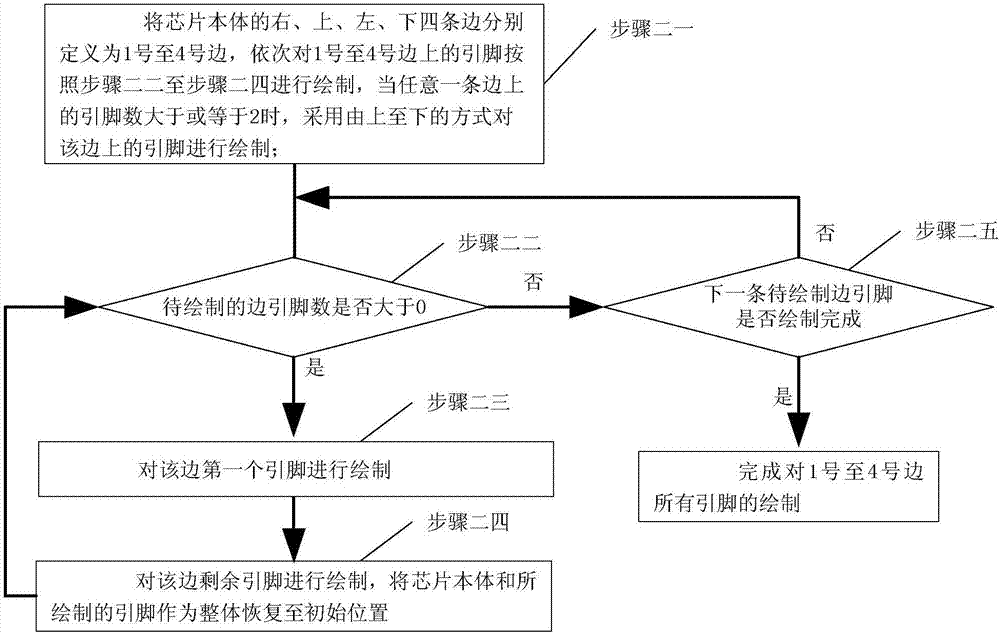
[0034] Step 21: Define the right, upper, left, and lower sides of the chip body as sides No. 1 to No. 4, and use the openGL graphics program interface function for the pins on sides No. 1 to No. 4 in turn. Step 2 and 4 draw, when the number of pins on any side is greater than or equal to 2, draw the pins on the side from top to bottom;
[0035]Step 2 and 2: judge whether the number of side pins to be drawn is greater than 0, if the judgment result is yes, perform steps 2 and 3, if the judgme...
PUM
 Abstract
Description
Claims
Application Information
 - Generate Ideas
- Intellectual Property
- Life Sciences
- Materials
- Tech Scout
- Unparalleled Data Quality
- Higher Quality Content
- 60% Fewer Hallucinations
Browse by: Latest US Patents, China's latest patents, Technical Efficacy Thesaurus, Application Domain, Technology Topic, Popular Technical Reports.
© 2025 PatSnap. All rights reserved.Legal|Privacy policy|Modern Slavery Act Transparency Statement|Sitemap|About US| Contact US: help@patsnap.com