
Array substrate, manufacturing method thereof, and display device

A technology for an array substrate and a manufacturing method, which is applied in the fields of array substrates and their manufacturing methods and display devices, and can solve problems such as difficulty in detecting line defects, short-circuiting of data lines, and decline in product yield, so as to reduce the probability of occurrence of line defects , to ensure the display effect and improve the yield rate

Active Publication Date: 2020-05-01
BOE TECH GRP CO LTD +1
View PDF2 Cites 0 Cited by
  • Summary
  • Abstract
  • Description
  • Claims
  • Application Information

AI Technical Summary

Problems solved by technology

Since the distance between the grid line and the data line at the overlapping area where the grid line and the data line are projected on the substrate is small, if a hillock is generated between the grid line and the data line at the overlapping area, then It is easy to cause the gate line and the data line in the overlapping area to be short-circuited, forming a line defect, and the size of the hillock is usually less than 1 micron, which is difficult to observe even under a microscope, making the detection of line defects very difficult
[0004] Therefore, in the prior art, the hillock generated between the gate line and the data line at the overlapping area where the gate line and the data line are projected on the substrate is likely to cause a short circuit between the gate line and the data line at the overlapping area. , forming line defects, leading to a decrease in product yield and affecting the display effect of the product

Method used


Image

  • Array substrate, manufacturing method thereof, and display device
  • Array substrate, manufacturing method thereof, and display device
  • Array substrate, manufacturing method thereof, and display device

Examples


Embodiment Construction

[0040] In order for those skilled in the art to better understand the technical solution of the present invention, the array substrate, its manufacturing method and display device provided by the present invention will be described in detail below with reference to the accompanying drawings.

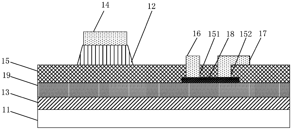
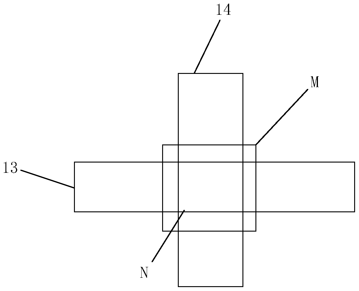
[0041] figure 1 It is a schematic structural diagram of an array substrate provided in Embodiment 1 of the present invention, figure 2 It is the top view of the middle spacer layer, the first conductive pattern layer and the second conductive pattern layer in embodiment one, as figure 1 and figure 2 As shown, the array substrate includes a base substrate 11 and a spacer layer 12 located on the base substrate 11, a first conductive pattern layer and a second conductive pattern layer, and the spacer layer 12 is arranged on the first conductive pattern layer and the second conductive pattern layer between the layers, and the projection M of the spacer layer 12 on the substrate 11 covers...


PUM


Abstract

The present invention provides an array substrate, a manufacturing method thereof and a display device. The array substrate includes a base substrate and a spacer layer on the base substrate, a first conductive pattern layer and a second conductive pattern layer. The spacer layer is disposed between the first conductive pattern layer and the second conductive layer; and the projection of the spacer layer on the base substrate covers a projected overlapping area of the first conductive pattern layer and the second conductive pattern layer on the base substrate. The present invention avoids the short circuit between the conductive pattern layers that are easily caused when the hillocks are formed between the first conductive pattern layer and the second conductive pattern layer at the overlapped area and reduces the probability of the occurrence of the line defects so as to improve the display panel yield and to ensure the display of the product.

Description

technical field [0001] The present invention relates to the field of display technology, in particular to an array substrate, a manufacturing method thereof, and a display device. Background technique [0002] In the traditional manufacturing process of the organic light-emitting diode (Organic Light-Emitting Diode, referred to as: OLED) backplane, the thick aluminum process is often used to manufacture the gate lines. [0003] Since the thermal expansion coefficient of aluminum itself is relatively large, hillocks are likely to be formed on aluminum at high temperatures (about 300° C.). In the backplane process, the temperature generated in the production of the insulating layer and the annealing process is much higher than 300°C, and because the thick aluminum process is used to make the grid lines, the probability of hillocks in the backplane process is greatly increased. . Since the distance between the grid line and the data line at the overlapping area where the grid...

Claims


Application Information

Patent Timeline
Patent Type & Authority Patents(China)
IPC IPC(8): H01L27/12H01L21/77
CPCH01L27/124H01L27/1259
Inventor 蔡振飞徐攀潘鑫袁粲袁志东
Owner BOE TECH GRP CO LTD
Learn More