
Organic light emitting display panel and organic light emitting display device

A light-emitting display, organic technology, applied in semiconductor devices, electrical components, circuits, etc., can solve problems such as reducing the yield of white light organic light-emitting display panels, reducing the service life of organic light-emitting display panels, and increasing the manufacturing process of organic light-emitting display panels. , to achieve the effect of reducing process complexity, improving service life and improving display accuracy

Active Publication Date: 2017-11-07
WUHAN TIANMA MICRO ELECTRONICS CO LTD
View PDF6 Cites 9 Cited by
  • Summary
  • Abstract
  • Description
  • Claims
  • Application Information

AI Technical Summary

Problems solved by technology

This increases the manufacturing process of organic light-emitting display panels and reduces the yield rate of white light organic light-emitting display panels.
[0003] At the same time, the blue light-emitting layer in the prior art will lead to a significant decrease in the brightness of the blue light with the prolongation of the use time. In order to improve the stability of the blue light brightness, the current density of the blue pixel is usually increased. In this way, the organic light will be further reduced. Service life of illuminated display panels

Method used


Image

  • Organic light emitting display panel and organic light emitting display device
  • Organic light emitting display panel and organic light emitting display device
  • Organic light emitting display panel and organic light emitting display device

Examples


Embodiment Construction

[0031] The application will be further described in detail below in conjunction with the accompanying drawings and embodiments. It should be understood that the specific embodiments described here are only used to explain the related application, not to limit the application. In addition, it should be noted that, for ease of description, only parts relevant to the present application are shown in the drawings.

[0032] It should be noted that, in the case of no conflict, the embodiments in the present application and the features in the embodiments can be combined with each other. The present application will be described in detail below with reference to the accompanying drawings and embodiments.

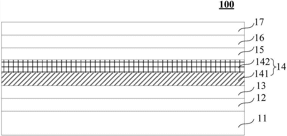
[0033] Please refer to figure 1 , which shows a schematic structural view of an organic light emitting display panel provided by the present application.

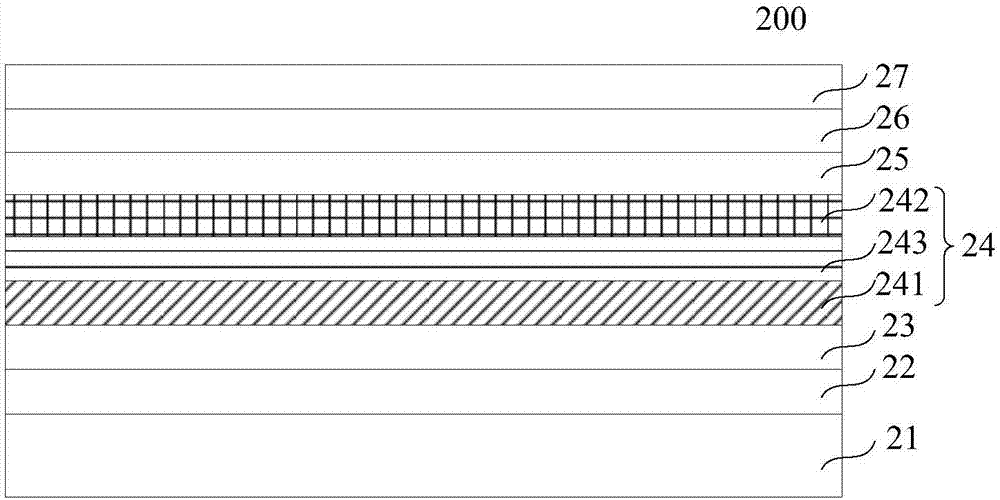
[0034] Such as figure 1 The organic light-emitting display panel 100 shown includes a base substrate 11, wherein the base ...


PUM


Abstract

The invention discloses an organic light emitting display panel and an organic light emitting display device. The organic light emitting display panel comprises a substrate, and a first electrode, a first transmission layer, an organic light emitting layer, a second transmission layer and a second electrode sequentially arranged on the substrate, wherein the organic light emitting layer comprises a blue light-emitting layer and a sapphire light-emitting layer. The wavelength scope of the blue light emitted by the blue light-emitting layer is 460nm-490nm, and the wavelength scope of the sapphire light emitted by the sapphire light-emitting layer is 425nm-455nm. The organic light emitting display panel further comprises a chroma adjustment layer which is arranged on one side of the second electrode away from the substrate, and the chroma adjustment layer is used for adjusting the light emitted from the second electrode. A blue light-emitting layer and a sapphire light-emitting layer improve the light extracting rate of the organic light emitting display panel and prolong the service lifetime of the organic light emitting layer. The display effect of the organic light emitting display panel is improved.

Description

technical field [0001] The present invention generally relates to the field of display technology, and in particular to an organic light emitting display panel and an organic light emitting display device. Background technique [0002] In the existing organic light emitting display panel technology, in order to obtain white light emitted from the organic light emitting display panel, the organic light emitting layer in the organic light emitting display panel is usually provided with three layers of blue light emitting layer, red light emitting layer and green light emitting layer, and at the same time A charge generation layer is arranged between every two light-emitting layers, and white light is formed by changing the luminous efficiency and brightness ratio of the three-color light-emitting layers. This increases the manufacturing process of the organic light emitting display panel and reduces the yield rate of the white light organic light emitting display panel. [00...

Claims


Application Information

Patent Timeline
Patent Type & Authority Applications(China)
IPC IPC(8): H01L51/50H01L27/32
CPCH10K59/00H10K50/115H10K50/131H10K50/125H10K50/11
Inventor 马洪虎牛晶华王湘成
Owner WUHAN TIANMA MICRO ELECTRONICS CO LTD
Learn More