Wafer processing method

A processing method and wafer technology, applied in metal processing equipment, manufacturing tools, laser welding equipment, etc., can solve the problems of meandering cuts and inability to grow cracks

Active Publication Date: 2022-02-11
DISCO CORP
View PDF5 Cites 1 Cited by
  • Summary
  • Abstract
  • Description
  • Claims
  • Application Information

AI Technical Summary

Problems solved by technology

[0004] However, in recent years, in order to improve the electrical characteristics, silicon wafers and the like whose crystal orientation has an angle of 45° with respect to the planned dividing line are widely used. Cuts meander near the corners of the device
The reason for this is considered to be that the cracks from the modified layer to the front face cannot grow smoothly along the planned dividing line because the modified layer is formed in a dotted line shape.

Method used


Image

  • Wafer processing method
  • Wafer processing method
  • Wafer processing method

Examples


Embodiment Construction

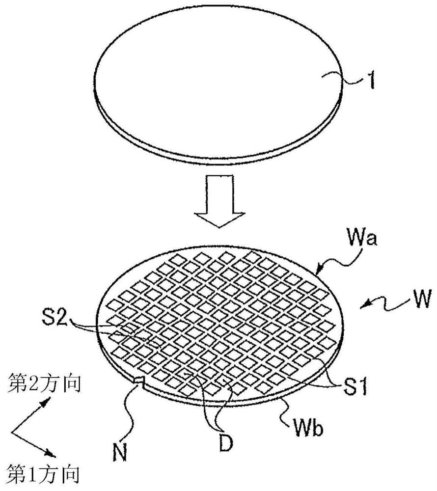
[0021] figure 1 The illustrated wafer W is an example of a workpiece having a circular plate-shaped substrate. On the front surface Wa of the wafer W, devices D are formed in a plurality of regions divided by a plurality of first planned dividing lines S1 and a plurality of second planned dividing lines S2, wherein the plurality of first planned dividing lines S1 The plurality of second planned division lines S2 extend in a second direction intersecting the plurality of first planned division lines S1 , for example, in a predetermined direction, such as a first direction. On the other hand, the surface of the wafer W opposite to the front surface Wa becomes the back surface Wb to be ground. The wafer W is, for example, a silicon wafer whose crystal orientation has an angle of 45° with respect to the extending direction of the first planned dividing line S1 and the second planned dividing line S2, and has a crystal orientation oriented at 45° with respect to the crystal orient...


PUM


Abstract

Provides a wafer processing method that prevents notches from forming at the corners of the device or meandering of the kerf near the corners. Regarding the processing method of the wafer, in the first modified layer forming step or in the second modified layer forming step, or in the two steps of the first modified layer forming step and the second modified layer forming step, forming The modified layer (M) inside the wafer (W) is formed compositely of at least one induced modified layer (Mi) and at least one adjusted modified layer (Ma) per one planned dividing line , the inducing modified layer induces the growth of cracks from the modified layer to the front side (Wa) of the wafer, and the adjustment modified layer is used to adjust the growth of cracks from the modified layer to the front side of the wafer, so it can Cracks generated from the modified layer are induced to the front side of the wafer by inducing the modified layer, and growth of cracks reaching the front side is adjusted by adjusting the modified layer, so that the wafer can be favorably divided into individual devices.

Description

technical field [0001] The present invention relates to a method of processing a wafer, which is divided into individual devices. Background technique [0002] After the modified layer is formed inside the wafer, the device is formed into chips while being ground. In the above process, the devices may contact each other due to the movement of the devices after the singulation during grinding, and defects may be generated at the corners of the devices. The problem. This problem is caused by movement when the device is singulated. Therefore, in order to adjust the timing of singulation in order to adjust the growth of cracks from the modified layer to the front surface, there is a processing method in which the inside of the wafer is irradiated with laser beams for forming the modified layer in a dotted line shape (e.g. , refer to the following patent document 1). [0003] Patent Document 1: Japanese Patent Laid-Open No. 2014-33163 [0004] However, in recent years, in ord...

Claims


Application Information

Patent Timeline
Patent Type & Authority Patents(China)
IPC IPC(8): H01L21/78B23K26/00
CPCH01L21/78B23K26/00H01L21/6836H01L21/76H01L21/268
Inventor 裵泰羽
Owner DISCO CORP
Why Eureka
Try Eureka