
Display panel and display

A display panel and substrate technology, applied in the direction of instruments, nonlinear optics, optics, etc., can solve problems affecting the quality of liquid crystal display panels, reduce the aperture ratio of liquid crystal display panels, etc., achieve small dimensional errors, increase aperture ratio, and high quality Effect

Inactive Publication Date: 2017-10-13
WUHAN CHINA STAR OPTOELECTRONICS TECH CO LTD
View PDF6 Cites 16 Cited by
  • Summary
  • Abstract
  • Description
  • Claims
  • Application Information

AI Technical Summary

Problems solved by technology

In order to prevent light leakage from the edges of the main spacer and the sub-spacer, it is necessary to make a large enough black matrix (Black Matrix, BM) at the bottom of the main spacer and the sub-spacer for light shielding, which will reduce the size of the liquid crystal display panel. Aperture ratio, which affects the quality of the LCD panel

Method used


Image

  • Display panel and display
  • Display panel and display
  • Display panel and display

Examples


Embodiment Construction

[0032] The technical solutions in the embodiments of the present invention will be described below in conjunction with the accompanying drawings in the embodiments of the present invention. Obviously, the described embodiments are only some of the embodiments of the present invention, not all of them. Based on the embodiments of the present invention, all other embodiments obtained by persons of ordinary skill in the art without creative efforts fall within the protection scope of the present invention.

[0033] In addition, the following descriptions of the various embodiments refer to the attached drawings to illustrate specific embodiments in which the present invention can be implemented. The directional terms mentioned in the present invention, for example, "upper", "lower", "front", "rear", "left", "right", "inner", "outer", "side", etc., only is to refer to the direction of the attached drawings. Therefore, the direction terms used are for better and more clearly explai...


PUM


Abstract

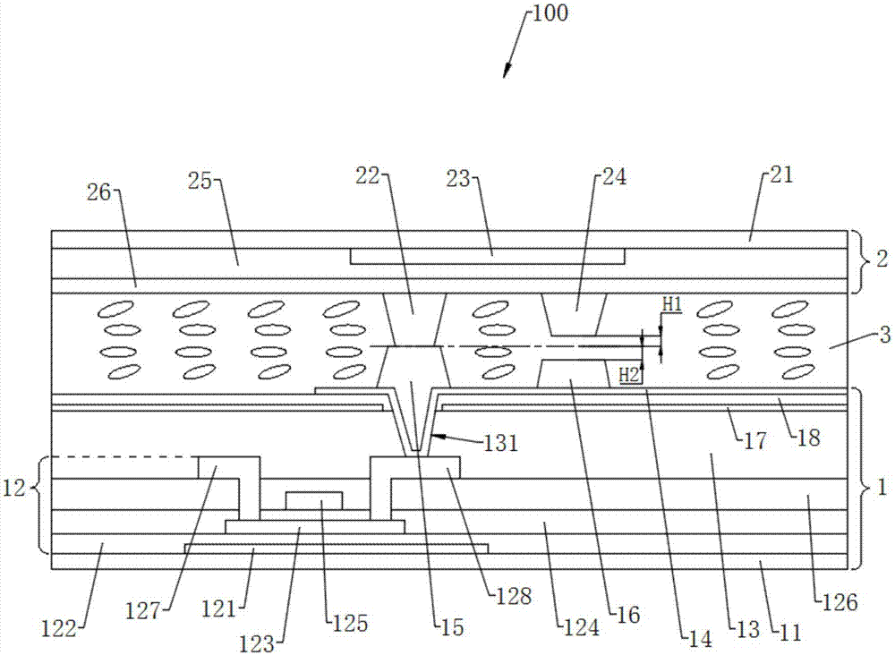
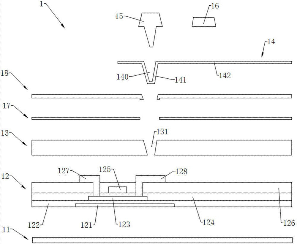
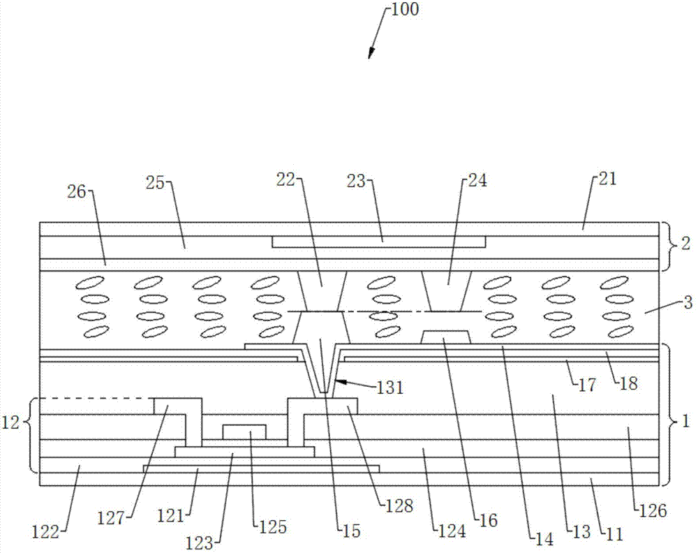
The invention discloses a display panel. The display panel comprises an array substrate and a color film substrate. The array substrate and the color film substrate are arranged oppositely. The array substrate comprises a first substrate body, a thin-film transistor device layer, a flat layer, a pixel electrode and a main holder, wherein the first substrate body, the thin-film transistor device layer and the flat layer are arranged in a laminated mode, and the flat layer is provided with a through hole; the pixel electrode is located at the side, away from the thin-film transistor device layer, of the flat layer, and is connected to the thin-film transistor device layer through the through hole; the main holder is located at the side, away from the flat layer, of the pixel electrode. The color film substrate comprises a second substrate body, a main spacer and a black matrix, wherein the second substrate body is arranged opposite to the first substrate body, the main spacer is located between the first substrate body and the second substrate body and abuts against the main holder, and the black matrix is arranged on the second substrate body and is located between the main spacer and the second substrate body, and covers an orthographic projection of the main spacer on the second substrate body. The aperture opening ratio of the display panel is high. The invention further discloses a display.

Description

technical field [0001] The present invention relates to the technical field of display devices, in particular to a display panel and a display. Background technique [0002] A Liquid Crystal Display (LCD) has many advantages such as a thin body, power saving, and no radiation, and has been widely used. Such as: LCD TV, mobile phone, personal digital assistant (PDA), digital camera, computer screen or laptop screen, etc. [0003] Generally, a liquid crystal display includes a housing, a liquid crystal display panel disposed in the housing, and a backlight module disposed in the housing. Among them, the structure of the liquid crystal display panel is mainly composed of a thin film transistor array (Thin Film Transistor Array, TFT Array) substrate, a color filter (Color Filter, CF) substrate, and a liquid crystal layer (Liquid Crystal Layer) arranged between the two substrates. ), its working principle is to control the rotation of the liquid crystal molecules in the liquid ...

Claims


Application Information

Patent Timeline
Patent Type & Authority Applications(China)
IPC IPC(8): G02F1/1339
CPCG02F1/13394
Inventor 邬金芳李亚锋
Owner WUHAN CHINA STAR OPTOELECTRONICS TECH CO LTD
Learn More