Pixel structure
A pixel structure, pixel technology, applied in nonlinear optics, instruments, optics, etc., can solve the problems to be strengthened, and achieve the effect of improving the color shift problem
- Summary
- Abstract
- Description
- Claims
- Application Information
AI Technical Summary
Problems solved by technology
Method used
Image
Examples
Embodiment Construction
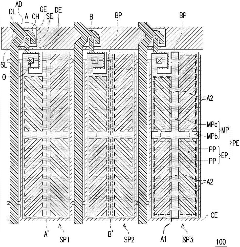
[0096] Figure 1A is a schematic top view of a pixel structure according to the first embodiment of the present invention, wherein Figure 1A Partial film layers are omitted. Figure 1B and Figure 1C are along Figure 1A Schematic cross-sectional view of the middle line A-A', B-B'. Please refer to Figure 1A to Figure 1C , the pixel structure 100 of this embodiment includes a plurality of sub-pixels arranged in an array, such as a first sub-pixel SP1, a second sub-pixel SP2 and a third sub-pixel SP3. The sub-pixels are arranged, for example, on the substrate SUB. In addition, a plurality of scanning lines SL may be further arranged on the substrate SUB ( Figure 1A Only one scan line SL) and multiple data lines DL are schematically shown. The scan lines SL and the data lines DL intersect with each other to define the area where each sub-pixel SP is located. In addition, each sub-pixel is suitable to be driven by one of the scan lines SL and one of the data lines DL.
[0...
PUM
 Abstract
Description
Claims
Application Information
 - R&D Engineer
- R&D Manager
- IP Professional
- Industry Leading Data Capabilities
- Powerful AI technology
- Patent DNA Extraction
Browse by: Latest US Patents, China's latest patents, Technical Efficacy Thesaurus, Application Domain, Technology Topic, Popular Technical Reports.
© 2024 PatSnap. All rights reserved.Legal|Privacy policy|Modern Slavery Act Transparency Statement|Sitemap|About US| Contact US: help@patsnap.com


