A kind of nand Flash voltage automatic compensation method and device
An automatic compensation and voltage technology, applied in information storage, static memory, instruments, etc., can solve problems such as threshold voltage range shift, wrong judgment and change of CELL data, avoid misjudgment and improve data reading and writing accuracy Effect
- Summary
- Abstract
- Description
- Claims
- Application Information
AI Technical Summary
Problems solved by technology
Method used
Image
Examples
Embodiment 1
[0047] A method for automatic voltage compensation of NAND Flash provided by an embodiment of the present invention is introduced in detail.
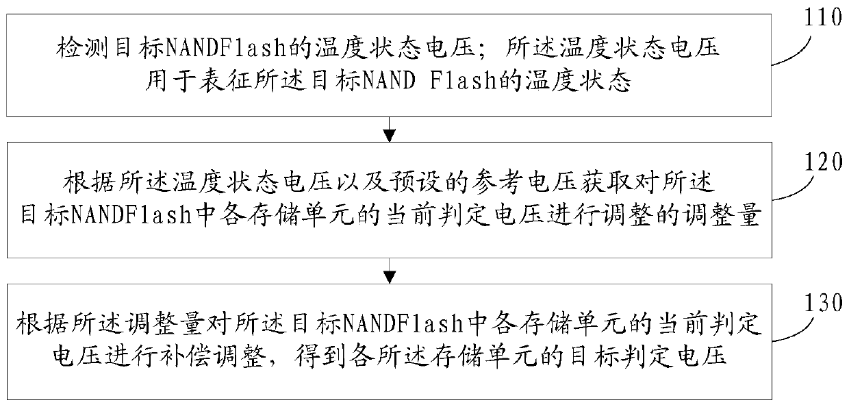
[0048] refer to figure 1 , shows a flow chart of the steps of a method for automatic voltage compensation of NAND Flash in an embodiment of the present invention.
[0049] Step 110, detecting the temperature state voltage of the target NAND Flash; the temperature state voltage is used to characterize the temperature state of the target NAND Flash.
[0050] Step 120, obtaining an adjustment amount for adjusting the current determination voltage of each storage unit in the target NAND Flash according to the temperature state voltage and a preset reference voltage.
[0051] Step 130: Compensate and adjust the current judgment voltage of each memory cell in the target NAND Flash according to the adjustment amount, so as to obtain the target judgment voltage of each memory cell.
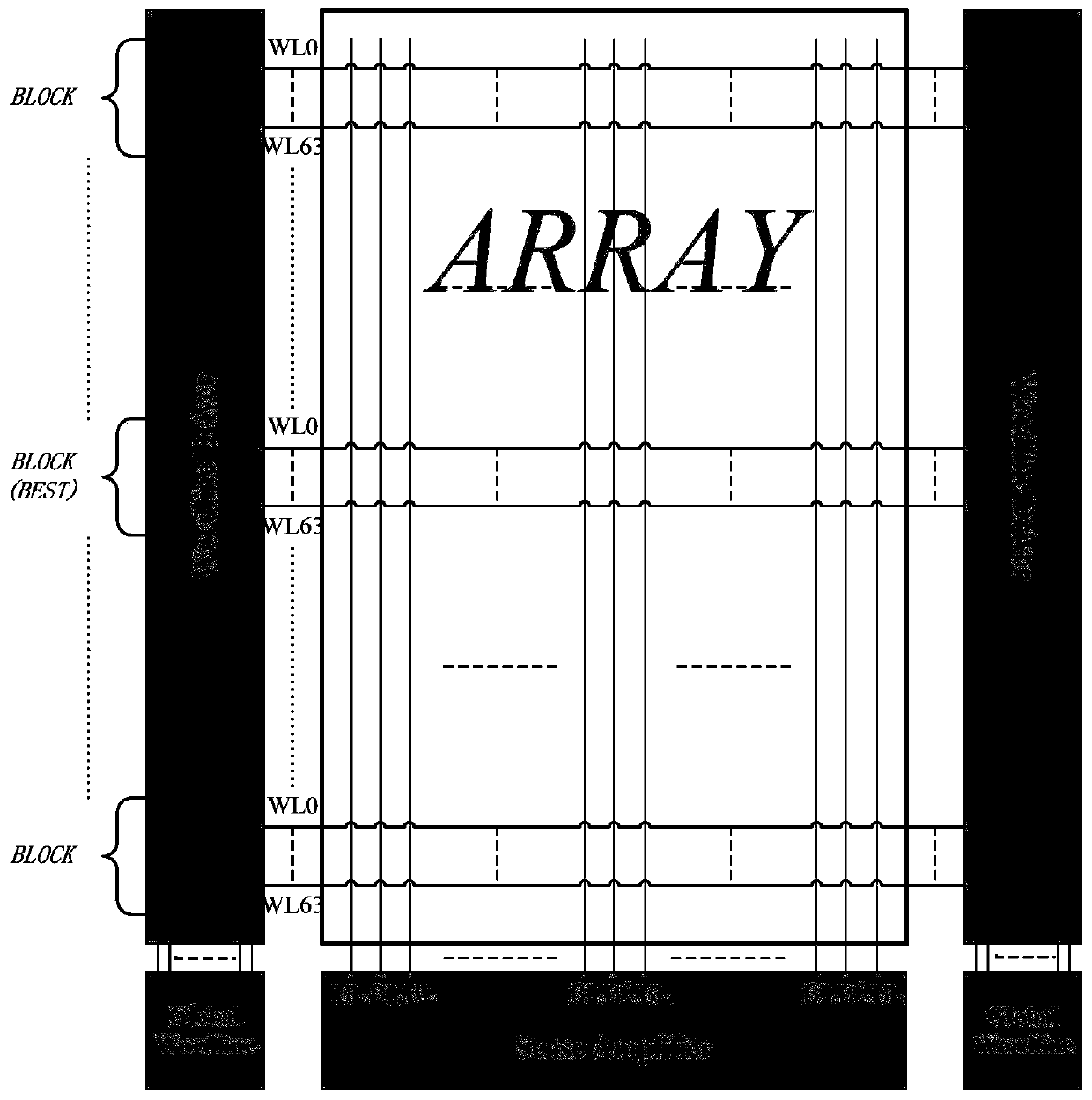
[0052] like Figure 1A It is an array organization structu...
Embodiment 2
[0076] A method for automatic voltage compensation of NAND Flash provided by an embodiment of the present invention is introduced in detail.
[0077] refer to figure 2 , shows a flow chart of the steps of a method for automatic voltage compensation of NAND Flash in an embodiment of the present invention.
[0078] Step 210, detecting the temperature state voltage of the target NAND Flash; the temperature state voltage is used to characterize the temperature state of the target NAND Flash; the temperature state voltage is proportional to the temperature of the target NAND Flash.
[0079] Step 220, calculating a first difference between the temperature state voltage and the reference voltage.
[0080] Step 230, performing analog-to-digital conversion on the first difference to obtain an adjustment amount for adjusting the current determination voltage of each memory cell in the target NAND Flash.
[0081] In this application, the first difference between the detected temperatu...
Embodiment 3
[0092] A method for automatic voltage compensation of NAND Flash provided by an embodiment of the present invention is introduced in detail.
[0093] refer to image 3 , shows a flow chart of the steps of a method for automatic voltage compensation of NAND Flash in an embodiment of the present invention.
[0094] Step 310, detecting the temperature state voltage of the target NAND Flash; the temperature state voltage is used to characterize the temperature state of the target NAND Flash; the temperature state voltage is inversely proportional to the temperature of the target NAND Flash.
[0095] Step 320, calculating a first difference between the temperature state voltage and the reference voltage.
[0096] Step 330, performing analog-to-digital conversion on the first difference to obtain an adjustment amount for adjusting the current determination voltage of each memory cell in the target NAND Flash.
[0097] Step 340, for each storage unit in the target NAND Flash, calcu...
PUM
 Abstract
Description
Claims
Application Information
 - R&D
- Intellectual Property
- Life Sciences
- Materials
- Tech Scout
- Unparalleled Data Quality
- Higher Quality Content
- 60% Fewer Hallucinations
Browse by: Latest US Patents, China's latest patents, Technical Efficacy Thesaurus, Application Domain, Technology Topic, Popular Technical Reports.
© 2025 PatSnap. All rights reserved.Legal|Privacy policy|Modern Slavery Act Transparency Statement|Sitemap|About US| Contact US: help@patsnap.com


