Touch substrate and touch display panel

A substrate and touch technology, applied in the direction of instruments, electrical digital data processing, data processing input/output process, etc., can solve the problems of waste of materials, affecting the capacitance of touch electrode blocks, and uneven capacitance of touch display panels , to achieve the effect of uniform capacitance

Active Publication Date: 2017-09-15
BOE TECH GRP CO LTD +1
View PDF9 Cites 5 Cited by
  • Summary
  • Abstract
  • Description
  • Claims
  • Application Information

AI Technical Summary

Problems solved by technology

[0003] The capacitive touch panel is an important form of the touch panel. In the existing touch display panel, there are various metal wiring arrangements on the other three sides except the driving circuit side (IC side), which will cause Parasitic capacitance, which affects the capacitance of the touch electrode blocks on each side of the touch display panel, and then causes the overall capacitance of the touch display panel to be uneven, affecting product yield, and also causing waste of materials

Method used


Image

  • Touch substrate and touch display panel

Examples


Embodiment 1

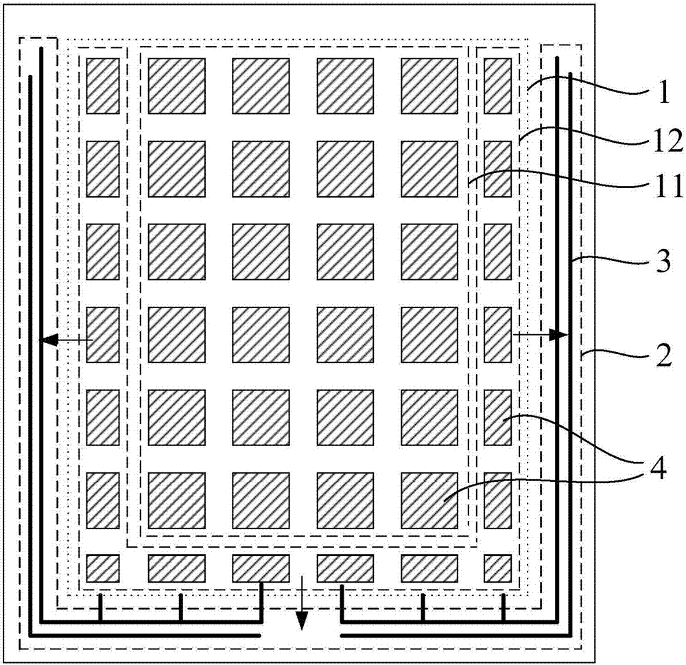
[0024] Such as figure 1 As shown, this embodiment provides a touch substrate, which includes a touch area 1 and a wiring area 2 located outside at least part of the side of the touch area 1; The signal line 3; the touch area 1 is divided into an additional sensing area 12 adjacent to the wiring area 2 and a normal sensing area 11 except for the additional sensing area 12, and both the additional sensing area 12 and the normal sensing area 11 are equipped with A plurality of touch electrode blocks 4 , wherein the area of ​​each touch electrode block 4 in the additional sensing area 12 is smaller than the area of ​​each touch electrode block 4 in the normal sensing area 11 .

[0025] The touch substrate has a touch area 1 for realizing the touch function, and many signal lines 3 (such as ground line GND, green signal line DG, etc.) in the touch substrate cannot be directly arranged in the touch area 1, but It should be arranged in the routing area 2 outside the touch area 1 , a...

Embodiment 2

[0049] This embodiment provides a touch display panel, including the touch substrate in Embodiment 1.

[0050] The touch display panel is preferably a self-contained in-cell (In-CELL) touch panel.

[0051] In the touch display panel provided by this embodiment, the area of ​​each touch electrode block in the additional sensing area is smaller than the area of ​​each touch electrode block in the normal sensing area, so that each touch electrode block in the additional sensing area The capacitance of the electrode blocks is smaller than the capacitance of each touch electrode block in the normal sensing area, and when the touch substrate is working, the capacitance of each touch electrode block in the additional sensing area is affected by the additional capacitance of the wiring area. Increase to the same capacitance as the touch electrode block in the normal sensing area, so that the capacitance of the touch electrode block on the touch substrate can be uniform without affecti...


PUM


Abstract

The invention provides a touch substrate and a touch display panel, belongs to the technical field of display, and solves the problem of non-uniform overall capacitance values of an existing touch display panel. The touch substrate comprises a touch region and a routing region located outside at least partial side edge of the touch region, wherein a signal line adjacent to the touch region is arranged in the routing region; the touch region is divided into an additional induction region adjacent to the routing region and a normal induction region except the additional induction region; a plurality of touch electrode blocks are arranged in each of the additional induction region and the normal induction region; and the area of each touch electrode block in the additional induction region is smaller than that of each touch electrode block of the normal induction region.

Description

technical field [0001] The invention belongs to the field of display technology, and in particular relates to a touch substrate and a touch display panel. Background technique [0002] With the development of technology, touch panels with touch control functions have gained more and more applications. [0003] Capacitive touch panel is an important form of touch panel. In the existing touch display panel, there are various metal wiring arrangements on the other three sides except the driving circuit side (IC side), which will cause The parasitic capacitance affects the capacitance of the touch electrode blocks on each side of the touch display panel, and then causes the overall capacitance of the touch display panel to be uneven, which affects the product yield and also causes waste of materials. Contents of the invention [0004] The purpose of the present invention is to at least solve one of the technical problems in the prior art, and to provide a touch control substr...

Claims


Application Information

Patent Timeline
Patent Type & Authority Applications(China)
IPC IPC(8): G06F3/041G06F3/044
CPCG06F3/0412G06F3/044
Inventor 尚建兴李森李晓东
Owner BOE TECH GRP CO LTD
Why Eureka
Try Eureka