Pixel circuit and driving method thereof and display device
A technology of pixel circuit and drive transistor, which can be applied to static indicators, instruments, etc., and can solve the problems of OLED life-span loss
- Summary
- Abstract
- Description
- Claims
- Application Information
AI Technical Summary
Problems solved by technology
Method used
Image

Examples
Embodiment 1
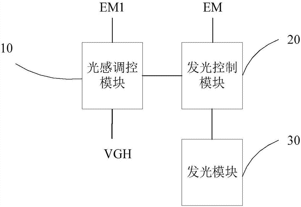
[0065] This embodiment provides a pixel circuit such as figure 1 As shown, the pixel circuit of this embodiment includes: a light sensing control module 10, a light emission control module 20 and a light emission module 30, wherein,
[0066] The light-sensing control module 10 is connected to the control signal terminal EM1, the first potential terminal VGH, and the light-emitting control module 20 respectively. The light-sensing control module 10 is used to receive the light from the light-emitting module 30, and generates corresponding electrical signals and signals according to the light intensity signal. Provide the signal of the first potential terminal VGH to the lighting control module 20 under the control of the regulation signal terminal EM1;
[0067] The light emission control module 20 is connected to the light emission control signal terminal EM, the light sensing control module 10 and the light emitting module 30 respectively, and the light emission control module...
Embodiment 2
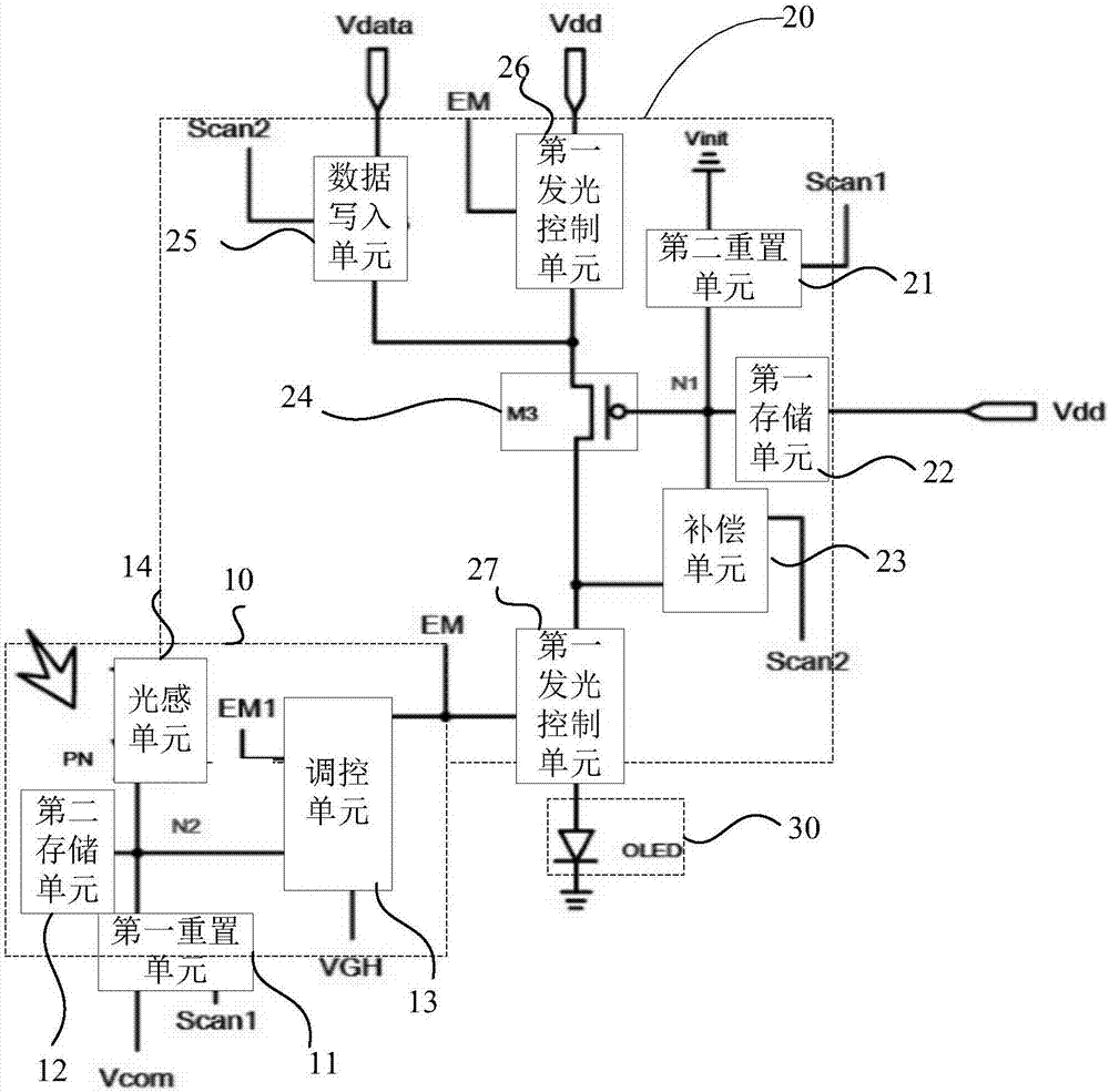
[0070] Such as figure 2 As shown, the photosensitive control module 10 in this embodiment includes: a first reset unit 11, a second storage unit 12, a control unit 13 and a photosensitive unit 14, wherein,
[0071] The first reset unit 11 is respectively connected to the first scanning signal terminal Scan1, the second potential terminal Vcom and the second node N2, and is used to provide the signal of the second potential terminal Vcom to the second node under the control of the first scanning signal terminal Scan1. Two nodes N2;
[0072] The second storage module 12 is respectively connected to the second node N2 and the second potential terminal Vcom; the second storage module 12 is used for charging or discharging under the control of the signal of the second node N2 and the signal of the second potential terminal Vcom;
[0073] The photosensitive unit 14 is respectively connected to the second node N2 and the low potential terminal Vss, the photosensitive unit 14 is use...
Embodiment 3
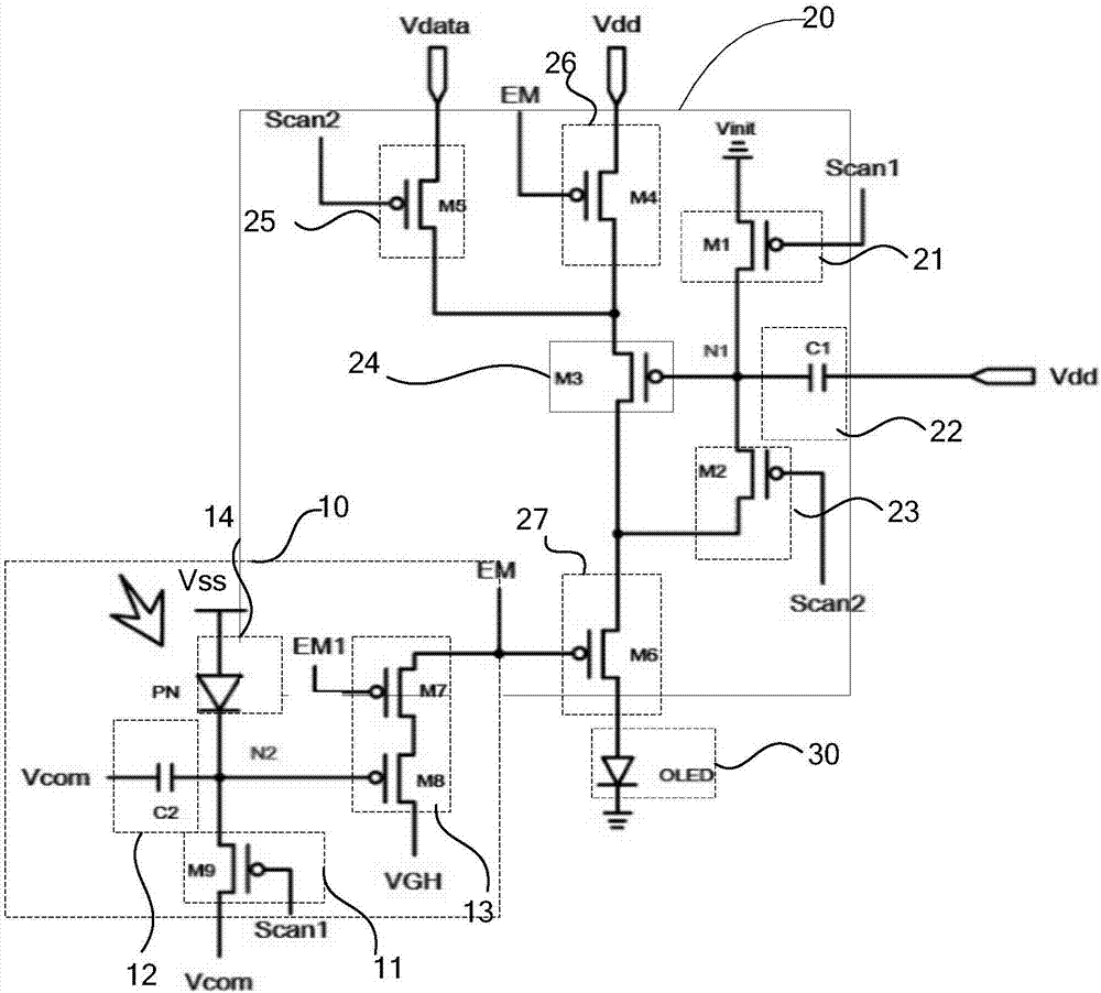
[0087] In specific implementation, in the above-mentioned pixel circuit provided by the embodiment of the present invention, as image 3 Shown:
[0088] The second reset unit 21 includes a first switching transistor M1, wherein the control electrode of the first switching transistor M1 is connected to the first scan signal terminal Scan1, the first electrode of the first switching transistor M1 is connected to the initialization signal terminal Vinit, and the first The second pole of the switching transistor M1 is connected to the first node N1.
[0089] The first storage unit 22 includes a first capacitor C1, wherein the first capacitor C1 is connected between the first node N1 and the third potential terminal Vdd.
[0090] The compensation unit 23 includes a second switch transistor M2, wherein the control electrode of the second switch transistor M2 is connected to the second scanning signal terminal Scan2, the first electrode of the second switch transistor M2 is connecte...
PUM
 Abstract
Description
Claims
Application Information
 - Generate Ideas
- Intellectual Property
- Life Sciences
- Materials
- Tech Scout
- Unparalleled Data Quality
- Higher Quality Content
- 60% Fewer Hallucinations
Browse by: Latest US Patents, China's latest patents, Technical Efficacy Thesaurus, Application Domain, Technology Topic, Popular Technical Reports.
© 2025 PatSnap. All rights reserved.Legal|Privacy policy|Modern Slavery Act Transparency Statement|Sitemap|About US| Contact US: help@patsnap.com